
1
ECE320L
Theory of Digital Systems
Laboratory Manual
California State University, Northridge
Prepared by: Soraya Roosta
Spring 2024

2
Table of Contents
Acknowledgment ............................................................................................................................ 3
Introduction .................................................................................................................................... 4
Experiment 1: Circuit Introduction with LEDs ................................................................................ 5
Experiment 2: Introduction to PSPICE and Logic Gate Simulation ............................................... 13
Experiment 3: Logic Gates and Pull-Up and Pull-Down Resistors ................................................ 35
Experiment 4: Boolean Laws And DeMorgan’s Theorems ........................................................... 41
Experiment 5: Logic Circuit Simplification .................................................................................... 53
Experiment 6: Half / Full Adder PSPICE Simulation ...................................................................... 60
Experiment 7: 2’s Complement Adder / Subtractor Circuit .......................................................... 77
Experiment 8: Multiplexers .......................................................................................................... 82
Experiment 9: Demultiplexer ........................................................................................................ 91
Experiment 10: D Latch and D Flip-Flop........................................................................................ 97
Experiment 11: J-K Flip-Flop ....................................................................................................... 107
Experiment 12: Asynchronous Counter ...................................................................................... 113
Experiment 13: Analysis of Synchronous Counters with Decoding ............................................ 123
Experiment 14: Design of Synchronous Counters ...................................................................... 131
Appendix A .................................................................................................................................. 136

3
Acknowledgment
I would like to thank Dr. George Law for providing his OrCAD based experiments. I would also
like to thank Dr. Ramin Roosta for reviewing the manual and his suggestions.
Special thanks to my T.A., Michael Granberry, for setting up the OrCAD for the experiments and
for his help in modifying the experiments.
I would also like to acknowledge the support and encouragement of Dr. Ashley Geng.

4
Introduction
HELLO STUDENTS
Welcome to the digital logic lab! In this lab, you will have the opportunity to experiment with and learn about
digital logic circuits. You will use a variety of equipment, such as power supplies, digital multimeters, function
generators, and oscilloscopes as well as software tools for simulating and modeling digital circuits.
The focus of this lab is to provide hands-on experience for students studying digital electronics and computer
engineering, allowing you to apply the theoretical concepts you have learned in class to real-world situations. You
will learn how to design, build, and test digital circuits using a variety of logic gates and other digital building
blocks.
Throughout the lab, you will work on a series of exercises and projects designed to help you understand the
fundamental principles of digital logic. These exercises will include basic logic gates, such as AND, OR, and NOT, as
well as more complex circuits like flip-flops and counters.
This lab will require a lot of time, effort, and attention to details, so be prepared by reviewing the materials before
coming to class. You will be working with equipment that can be fragile and expensive, so please handle it with
care.
You will also be required to keep a lab notebook (paper or electronic), where you will record your observations and
measurements, and to present the results of your work. Also, you will be required to turn in lab reports each week.
Let's get started and have a great time learning about digital logic!

5
Experiment 1: Circuit Introduction with LEDs
OJECTIVES
After completing this experiment, you will be able to:
• Use a DC power supply and DMM.
• Identify basic circuit components.
• Analyze a circuit containing a switch.
• Analyze a simple LED circuit and measure the forward voltage.
MATERIALS NEEDED
• One 330Ω
• Red, orange, yellow, green, blue, white LEDs
• 7404 hex inverter IC
THEORY
DIGITAL MULTIMETER (DMM)
A DMM, or Digital Multimeter, is a versatile electronic device used to measure various electrical quantities in a
simple and convenient way. A DMM typically has a digital display that shows numerical readings for measurements
such as voltage, current, resistance, and sometimes frequency.
GROUND
In a circuit, "ground" refers to a common reference point or voltage level against which other voltages are
measured. It serves as a point of reference for electrical potential and is typically designated as the zero-voltage
point. The circuit symbol for ground is shown in Figure 1.1.
Figure 1. 1
DC VOLTAGE SOURCE
A DC voltage source is a device that provides the appropriate DC voltage required by the device to function. 5
voltages (5V or +5.0V) are commonly used in digital systems. Two DC voltage source schematic symbols are shown
in Figure 1.2.
Figure 1. 2
RESISTOR
A resistor is an electronic component that limits the flow of electric current in a circuit. A resistor schematic
symbol is shown in Figure 1.3. The number next to the symbol tells the reader that the resistance is 330 ohms
(330Ω) or 1000 ohms (1kΩ). Sometimes the unit symbol ‘Ω’ is left out on schematics.
Figure 1. 3
+5.0V
+5.0V
330 1k

6
SWITCH
A switch, as shown in Figure 1.3, is a simple circuit component used to control the flow of electricity.
Figure 1. 4
It is typically used to manually open or close a circuit, allowing or preventing the current from flowing through the
circuit as shown in Figure 1.4.
Figure 1. 5: Switch Open and Switch Closed
Figure 1.4 shows another way to draw the circuits in Figure 1.5. This method is preferred in digital logic and will be
used throughout this lab manual. Typically, the positive voltages are towards the top of the schematic and ground
is at the bottom.
Figure 1. 6: Switch Open and Switch Closed
OHM’S LAW
When a voltage is applied across a resistor, the current flowing through the resistor can be calculated using to
Ohm's Law:
= =
O
hm's Law states that the current () flowing through a resistor is directly proportional to the voltage () applied
across it and inversely proportional to the resistance (
)
of the resistor.
EX
AMPLE 1.1
Find the current flowing through and the voltage across the 330Ω resister when the switch is closed and open.
SOLUTION
Since the DC voltage is V = 5V and the resistor has a resistance of R = 330Ω, therefore by Ohm’s Law:
=
=
5
= 15.15
= IR = (15.15mA)() 5V
C
A B
C
330
A
5V
330
5V
B
+5.0V
+5.0V
330
330
+5.0V
330

7
Thus, the current flowing through the circuit is 15.15 milliampere or 15.15mA. The voltage across the resistor is
equal to the DC voltage source. When the switch is open, = 0A, and therefore the voltage across the resistor is:
= 0 = 0A
(
)
When the switch is Open, node A has a voltage of 5V, and both nodes B and C have voltages of 0V. However, when
the switch is closed, both A and B are 5V and C remains at 0V. The voltage across the Resistors is the difference
between the voltage at Node B and at Node C.
V
BC
= V
B
– V
C
→ 5V
B
– 0V
C
= 5V
BC
.
Switch State
Node A, V
A
Node B, V
B
Node C, V
C
Node B to C, V
BC
Open
5V
0V
0V
0V
Closed
5V
5V
0V
5V
LED
A diode is an electronic component that allows electric current to flow in one direction while blocking it in the
opposite direction. It acts as a “one-way valve” for electrical current. The diode’s terminals are called the anode (+)
and cathode (-). An LED (Light-Emitting Diode) is a specific type of diode that emits light when current passes
through it. It is designed to convert electrical energy into light energy. The LED schematic symbol is show in Figure
1.6.
Figure 1. 7: LED
When the voltage across a diode is applied in the forward direction (anode connected to the positive terminal and
cathode connected to the negative terminal), it allows current to flow easily, similar to a closed switch. This is
known as the forward bias.
LED
Forward Voltage, V
f
Red 1.8V – 2.2V
Orange 2.0V – 2.2V
Yellow 2.0V – 2.2V
Green 2.0V – 3.5V
Blue 2.5V – 3.7V
White 2.5V – 3.7V
Table 1. 1: LED Forward Voltages
On the other hand, when the voltage is applied in the reverse direction (anode connected to the negative terminal
and cathode connected to the positive terminal), the diode blocks the current flow, acting as an open switch. This
is known as the reverse bias. NOTE: anode is the long leg and Cathode is the short leg.

8
Figure 1. 8: Circuit with LED and Resistor
EXAMPLE 1.2
Find the current flowing through the circuit if the LED has a forward voltage is V
f
= 2V.
SOLUTION
Since V = 5V, V
f
= 2V, and R = 330Ω, therefore by Ohm’s Law:
=
(
)
=
=
= 9.09.
Thus, the current flowing through the circuit is 9.09 milliampere or 9.09mA. Also note that the voltage across the
resistor is 3V.
5V = 2V + 3V.
PRELIMINARY PROCEDURE
1. Read the lab.
2. Research resistors, switches, LEDs, breadboards, DC power supplies, and logic gates. Briefly paraphrase your
findings. This will help you understand the topics presented in this lab. In addition, when you write your lab
report, use your research as the theory section of your report. You may include images, graphs, equations, etc.
330
330
Cathode (-)
5V
5V
Anode (+)
Cathode (-)
Anode (+)

9
PROCEDURE
1. Measure the resistance of one 330Ω and 1kΩ resistor. Record the measured values in Table 1.2. It’s a good
habit to measure your resistors’ values before you place them into your circuit.
Resistor, Ω Measured, Ω
330Ω
1kΩ
Table 1. 2
2. Build Figure 1.9 on a breadboard. If switches are not available, then one can emulate a switch by using a wire.
Measure and record the voltages across each resistor when the switch is open and closed. Observe that V
AB
+
V
BC
= V
AC
= V
Supply
when resistors are connected in series
.
Figure 2. 9
Switch State
Measured, V
Supply
Measured, V
AB
Measured, V
BC
Measured, V
AC
Open
Closed
Table 1. 3
3. Modify your circuit by replacing the 1kΩ resistor with an LED, as shown in Figure 1.10. Measure and record the
voltage across the resistor as well as the LED’s forward voltage, V
f
(anode to cathode). Observe that V
f +
V
R
=
V
DC
= 5V.
Figure 1. 10
Switch State Forward Voltage, V
f
Voltage across Resistor, V
R
LED State
(On or off)
Open
Closed
Table 1. 4
+5.0V
B
B
C
330
1k
5V
1k
A
330
C
A
Cathode (-) Cathode (-)
Anode (+)
+5.0V
330 330
Anode (+)
5V

10
4. Open the switch and insert your LED in the other direction so that it’s reverse bias. When the switch is closed,
is the LED on or off? Notice that V
rev
= V
Supply
= 5V when the switch is closed.
Figure 1. 11
Switch State Forward Voltage, V
rev
Voltage across Resistor, V
R
LED State
(On or off)
Open
Closed
Table 1. 5
5. Close the switch and turn the LED around so that the LED turns on. Measure the forward voltage and voltage
across the resistor for each LED color.
LED
Forward Voltage, V
f
Voltage across Resistor, V
R
Red
Orange
Yellow
Green
Blue
White
Table 1. 6
6. Connect two inverters in series (cascade) as shown in Figure 1.12. Check the logic when the input is connected
to 5V, open (not connected to anything), and 0V (Ground). Record your observations for these three cases in
Table 1.7.
Figure 1. 12
Wire State
LED 1, (On or off)
LED 2, (On or off)
5V
Open (Floating)
0V, Ground
Table 1. 7
Cathode (-)
Anode (+)
+5.0V
330
330
Anode (+)
5V
Cathode (-)
LED
7404
+5.0V
330330
1k
LED
7404

11
7. Connect the two inverters as cross-coupled inverters as shown in Figure 1.13. This is a basic latch circuit, the
most basic form of memory. This arrangement is not the best way to implement a latch but serves to illustrate
the concept (you will study latch circuits in more detail later). Check the logic when the input is connected to
5V, open (not connected to anything), 0V (Ground), and back to open. Record your observations for these
three cases in Table 1.8.
Figure 1. 13
Wire State
LED, (On or off)
5V
Open (Floating)
0V
Open (Floating)
Table 1. 8
1k
7404
LED
330
+5.0V
7404

12
EVALUATION AND REVIEW QUESTIONS
1. In Figure 1.9, we noticed that V
AB
+ V
BC
= V
AC
= V
DC
. Therefore, ohm’s law can be expanded to (V
AB
+ V
BC
) = (R
AB
+ R
BC
)(I). Find the current flowing through circuit. The same current flows through R
AB
and R
BC
.
2. Find the current flowing through circuit then the voltage across each resistor.
Figure 1. 14
3. According to your measurements in step 5, which LED has the least and most amount of current flowing
through it?
4. Find the current flowing through and the voltages across each resistor in Figure 1.15.
Figure 1. 15
5010k
5V 2.2k
7404
1k
330 330
+5.0V
7404
1k

13
Experiment 2: Introduction to PSPICE and Logic Gate Simulation
OJECTIVES
After completing this experiment, you will be able to
• Simulated the 7 fundamental logic gates on OrCAD PSPICE.
MATERIALS NEEDED
• OrCAD PSPICE
THEORY
ORCAD PSPICE:
In this experiment, we will simulate all 7 fundamental logic gates to gain familiarity with OrCAD PSPICE.
OrCAD PSpice is a software tool for simulating and analyzing the behavior of electronic circuits. It is a component
of the OrCAD electronic design automation (EDA) suite, which is used to design and manufacture electronic
systems and components.
PSpice provides a wide range of simulation models and analysis tools for analog, digital, and mixed-signal circuits.
It allows designers to analyze the performance of their circuits under different operating conditions and identify
potential issues before physically building and testing the circuits. The software has a graphical user interface (GUI)
that allows users to build and edit circuits using schematic capture and layout tools. It also includes a variety of
libraries of pre-defined components, such as transistors, resistors, capacitors, and integrated circuits, that can be
added to circuits.
PSpice is widely used in the electronics industry and academia for designing and testing electronic circuits,
including power supplies, amplifiers, filters, and controllers.
7 FUNDAMENTAL LOGIC GATES:
Digital logic gates are electronic circuits that perform logical operations on one or more input signals and produce
an output signal based on the logical operation. They are the basic building blocks of digital circuits and are used to
implement Boolean functions, which are mathematical functions that take in one or more input values and
produce a single output value.
There are several types of digital logic gates, including:
14
INVERTER
Figure 2. 1
Input
Output
X
Y
1
0
0
1
Table 2. 1
AND
Figure 2. 2
Input
Output
A
B
Y
0
0
0
0
1
0
1
0
0
1
1
1
Table 2. 2
OR
Figure 2. 3
Input
Output
A
B
Y
0
0
0
0
1
1
1
0
1
1
1
1
Table 2. 3
NAND
Figure 2. 4
Input
Output
A
B
Y
0
0
1
0
1
1
1
0
1
1
1
0
Table 2. 4
U11A
74LS04
1 2
U12A
74LS08
1
2
3
U3A
74LS32
1
2
3
U13A
74LS00
1
2
3

15
NOR
Figure 2. 5
Input
Output
A
B
Y
0
0
1
0
1
0
1
0
0
1
1
0
Table 2. 5
XOR
Figure 2. 6
Input
Output
A
B
Y
0
0
0
0
1
1
1
0
1
1
1
0
Table 2. 6
XNOR
Figure 2. 7
Input
Output
A
B
Y
0
0
1
0
1
0
1
0
0
1
1
1
Table 2. 7
U14A
74LS02
23
1
U15A
74LS86A
12
3
U8A
74LS266
1
2
3

16
PRELIMINARY PROCEDURE
1. Read the lab.
2. Draw the output waveform for each logic gate. We will use these results to compare with your PSPICE
simulations.
Table 2. 8

17
PROCEDURE
SIMULATING A NOT GATE IN PSPICE
STARTING A NEW PROJECT
1. Press File > New > Project to begin a new project.
Figure 2. 8
2. In the New Project window, title your file “FirstName-LastName-Lab1”, for example. Save it in a folder called
“Lab 1”. Check the box called Enable PSpice Simulation.
Figure 2. 9
3. In the Create PSpice Project pop-up window, select Create a blank project and Press OK.
Figure 2. 10
ADDING LIBRARIES
4. Press Place > Part or press P to bring up the parts library.

18
Figure 2. 11
5. In Place Part window, click the Add Library icon, . In the folder, open the library called 74LS, SOURCSTM.
Figure 2. 12
ADDING COMPONENTS TO SCHEMATIC
6. Now that your libraries are imported, select 74LS in the library window and search for 74LS04 by typing it in
the search window and press ENTER/RETURN on your keyboard.

19
Figure 2. 13
7. Drag your mouse over your schematic window and place the NOT gate on your schematic.
Figure 2. 14
8. In the SOURCSTM library, search for DigStim1 and add one to your schematic. Double click “Implementation”
text and type “X” in the Value textbox with Display Format set to Name and Value. Press OK.

20
Figure 2. 15
9. Add ports by going to Place > Hierarchical Port….
Figure 2. 16

21
10. Search for PORTLEFT-R in the CAPSYM library. Press OK. Place at the input of the NOT gate.
Figure 2. 17
11. Double click on the “PORTLEFT-R” text and rename it “X”.
Figure 2. 18

22
12. Similar for the output, place a PORTLEFT-L at the output of the NOT gate and rename it “out”.
Figure 2. 19
13. To connect the components together on the schematic with wires, go to Place > Wire or press W.
Figure 2. 20
14. Connect the components together in a similar manner as shown below.
Figure 2. 21
23
CREATING A NEW SIMULATION PROFILE
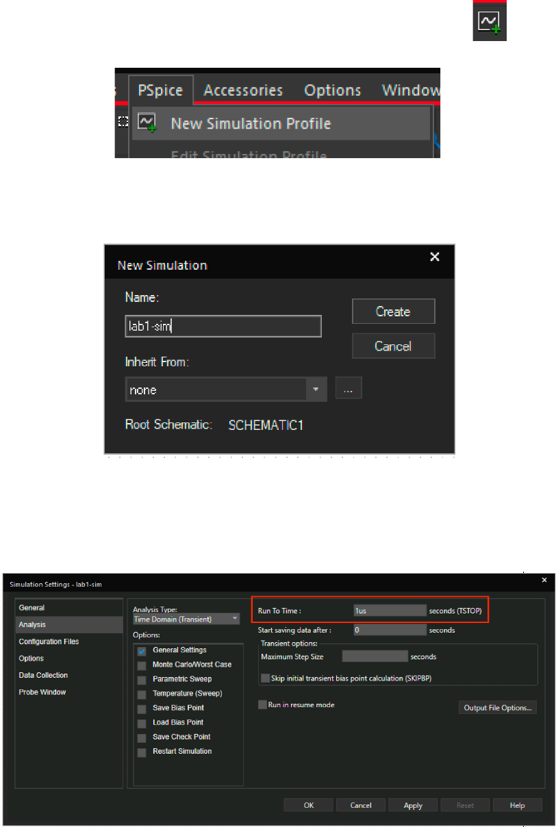
15. Create a new simulation profile by pressing PSpice > New Simulation Profile or click the icon.
Figure 2. 22
16. In the pop-up window type “lab1-sim”. Press Create when done. Leave Inherit From as none.
Figure 2. 23
17. A window called “Simulation Settings – lab1-sim” will pop-up. Set Run To Time to “1us”. This will make the
simulation run for 1us.
Figure 2. 24

24
18. Next, click on Options > Gate Level Simulation > General and set DIGINITSTATE to 0 under the Value column.
Then press Apply, then OK.
Figure 2. 25
CREATING A SIMULATION STIMULI
OrCAD Capture Lite offers several ways to create simulation stimuli. One way is to do it manually and another way
is to treat the inputs as if they are clocks. We will look at both methods this lab.
CREATE MANUALLY
19. Click the DSTM1 symbol to select the part so that a purple dotted rectangle encloses the part.
Figure 2. 26
20. Right click on the DSTM1 symbol and click Edit PSpice Stimulus.
Figure 2. 27

25
21. A New Stimulus window will pop up with “X” already in the Name text field. In the Digital section, select Signal,
then press OK.
Figure 2. 28
22. To add a new point or a transition to a stimulus, click the icon. Now, the arrow cursor symbol has
become a pencil symbol. Use this tool to toggle your input signal between 0 and 1. That is, once you have this
tool selected, click on the green signal to change the logic level. Toggle your signal from 0 to 1 at 0.5us. Your
final signals should look like the following.
Figure 2. 29
23. Press Save and press Yes to update schematic.
Figure 2. 30

26
RUN SIMULATION
24. Place Voltage Level markers schematic by going to PSPICE > Markers > Voltage Level or press icon.
Figure 2. 31
25. The Voltage Level markers must be placed on the wires.
Figure 2. 32

27
26. Press PSpice > Run or the icon to run simulation.
Figure 2. 33
27. Running the simulation will cause the Allegro PSpice Simulator program to open which will contain a
simulation of your schematic. It should look like the screenshot below.
Figure 2. 34
28. Press Trace > Cursor > Display or press to enable the cursor.
Figure 2. 35

28
29. This will let you see the level of your signal. Once enabled, left click and on your simulation to see the levels of
your signal. You can click hold and drag as well.
Figure 2. 36
30. Compare your simulated results with your pre-lab.
SIMULATING AN AND GATE IN PSPICE
The implementation and simulation for an AND gate is very similar to the NOT gate demonstrated previously.
STARTING A NEW PROJECT
1. Create a new project by going to File > New > New Project….
2. In the New Project window, name your project and save it in a new folder.
3. In the Create PSPICE Project window, click Create a black project, then press OK.
ADDING LIBRARIES
4. The necessary libraries should already be added to your library list from implementing the NOT gate. If not,
refer to step 2 in the from the previous section.
ADDING COMPONENTS TO SCHEMATIC
5. Open your parts window by pressing P and search for 74LS08 in the 74LS library. The 74LS08 is an AND gate.
Place the AND gate on your schematic. So far you should have the following:
Figure 1. 37
6. Place two DigStim1 parts on your schematic (one for each input). Double click on the “Implementation” text
and set the value to X and Y for each DigStim1.

29
7. Go to Place > Hierarchical Port… and place two PORTRIGHT-R ports to the left of the inputs of the AND gate.
Double click on the “PORTRIGHT-R” text and rename each port X and Y for each port.
8. Similarly, go to Place > Hierarchical Port… and place one PORTRIGHT-L port to the right of the output of the
AND gate. Double click on the “PORTLEFT-L” text and rename it out.
9. Press W for the wire tool and connect each component together with wires. So far you should have the
following:
Figure 2. 38
CREATING A NEW SIMULATION PROFILE
10. Create a new simulation profile by pressing PSpice > New Simulation Profile or click the icon.
11. In the pop-up window type “lab1-sim”. Press Create when done. Leave Inherit From as none.
12. A window called “Simulation Settings – lab1-sim” will pop-up. Set Run To Time to “1us”. This will make the
simulation run for 1us.
13. Next, click on Options > Gate Level Simulation > General and set DIGINITSTATE to 0 under the Value column.
Then press Apply, then OK.
CREATING A SIMULATION STIMULI
Now we will look at the second way to create simulation stimuli by treating the inputs as if they are clocks.
TREAT SIGNALS AS CLOCKS
14. Click the DSTM1 symbol to select the part so that a purple dotted rectangle encloses the part.
Figure 2. 39

30
15. Right click on the DSTM1 symbol and click Edit PSpice Stimulus from the menu.
Figure 2. 40
16. A New Stimulus window will pop up with “X” already in the Name text field. In the Digital section, select Signal,
then press OK.
Figure 2. 41

31
17. In the Clock Attributes window, set Specify by to Period and on time. Set Period (sec) to 160ns and On time
(sec) to 80ns. Press Apply, then OK.
Figure 2. 42
18. Set another stimulus for Y, press Stimulus > New….
Figure 2. 43
Figure 2. 44

32
19. In the Clock Attributes window, set Specify by to Period and on time. Set Period (sec) to 80ns and On time
(sec) to 40ns. Press Apply, then OK.
Figure 2. 45
20. Your Stimulus Editor should look like the following:
Figure 2. 46
21. Press Save and press Yes to update schematic.
Figure 2. 47

33
RUN SIMULATION
22. Place Voltage Level markers schematic by going to PSPICE > Markers > Voltage Level or press the icon.
The Voltage Level markers must be placed on the wires. Your schematic should look like the following:
Figure 2. 48
23. Press PSpice > Run or the icon to run simulation. Running the simulation will cause the Allegro PSpice
Simulator program to open which will contain a simulation of your schematic. It should look similar to the
screenshot below:
Figure 2. 49
24. Press Trace > Cursor > Display or press to enable the cursor. This will let you see the level of your signal.
Once enabled, left click and on your simulation to see the levels of your signal. You can click hold and drag as
well.
Figure 2. 50
25. Compare your simulated results with your pre-lab.
PRACTICE PSPICE
Here you will practice the steps above and simulate the remaining gates on your own.
Parts List in the 74LS library:
OR: 74LS32

34
Figure 2. 51
XOR: 74LS86A
Figure 2. 52
NAND:
Figure 2. 53
NOR:
Figure 2. 54
XNOR:
When you simulate the 74LS266, a ‘1’ will be simulated as a ‘Z’ (high impedance).
Figure 2. 55
For the remaining logic gates, compare your simulated results with your pre-lab.
U3A
74LS32
12
3
U2A
74LS86A
3
U13A
74LS00
1
2
3
U2A
74LS02
1
U1A
74LS266
3

35
Experiment 3: Logic Gates and Pull-Up and Pull-Down Resistors
OJECTIVES
After completing this experiment, you will be able to
• Experimentally verify the truth tables for the NAND and NOR, and inverter gates.
• Use the NAND and NOR gates to formulate other basic logic gates.
MATERIALS NEEDED
• 7400 quad 2-input NAND gate
• 7402 quad 2-input NOR gate
• 7404 NOT gate (inverter)
• DMM probes
THEORY
LOGIC GATES
Logic gates are the basic building blocks of digital electronic circuits. They are devices that perform a specific logic
operation on one or more input signals and produce a single output signal. The most basic logic gates are the NOT
gate, AND gate, OR gate, and XOR (exclusive OR) gate. These gates can be combined to create more complex
circuits that perform more advanced logic operations.
UNIVERSAL LOGIC GATES
There are three types of logic gates that are considered to be "universal" because they can be combined to create
any other logic gate or digital circuit. These universal gates are:
• NAND (NOT-AND) gate: This gate performs the opposite function of an AND gate, meaning it produces a
low output (0) if all of its inputs are high, and a high output (1) otherwise.
• NOR (NOT-OR) gate: This gate performs the opposite function of an OR gate, meaning it produces a high
output (1) if all of its inputs are low, and a low output (0) otherwise.
• NOT gate (inverter): As the name suggests, it inverts the input signal, so that a high input (1) produces a
low output (0), and vice versa.
• Since NAND and NOR gates are universal gates, any logic circuit can be implemented using only NAND
gates, or only NOR gates.
TTL (TRANSISTOR-TRANSISTOR LOGIC)
TTL (Transistor-Transistor Logic) is a type of digital logic circuit that uses transistors to switch between the two
logic levels of 0 and 1.
Figure 3. 1: TTL Switching Voltages

36
As shown in Figure 3.1, the logic HIGH or binary ‘1’ level is typically represented by a voltage between 2.4V-5V,
while the logic LOW or binary ‘0’ level is represented by a voltage between 0V-0.4V. The exact voltage levels may
vary depending on the specific type of TTL circuit.
HOW TO CREATE INPUT SIGNALS IN THE LAB
Pull-down and pull-up resistors are used in electronic circuits to establish a known or defined voltage level when a
switch is open. They are typically used in digital circuits to prevent floating or undefined states that could lead to
unreliable or incorrect readings.
Figure 3. 2
PULL-DOWN RESISTOR
A pull-down resistor is connected between the signal line and ground. When the switch is open, the pull-down
resistor ensures that the voltage is “pulled down” to a LOW level (e.g., 0 volts or ground). This establishes a clear
"off" or "0" state for the signal.
PULL-UP RESISTOR
On the other hand, a pull-up resistor is connected between the signal line and a positive voltage source (e.g., Vcc
or +5 volts). When the switch is open, the pull-up resistor “pulls” the voltage up to a high level (e.g., 5 volts). This
establishes a clear "on" or "1" state for the signal.
When the switch is closed, the pull-down or pull-up resistor has little effect as the switch takes precedence and
overrides the resistor's influence on the signal voltage level.
V
in
Switch State
Pull-Down
Pull-Up
Open
0V, ‘0’
5V, ‘1’
Closed
5V, ‘1’
0V, ‘0’
Table 3. 1
In digital circuits, it's important to have a well-defined voltage level to ensure reliable signal interpretation by the
receiving circuitry (such as microcontrollers or logic gates).
NAMING PORTS ON A SCHEMATIC
To simplify the schematic, we can replace the entire pull-up or pull-down network with just the port.
Figure 3. 3
1k, Pull-Down
Vout
+5.0V
+5.0V
1k, Pull-Up
Vout
1k
Vin
A
+5.0V
A

37
PRELIMINARY PROCEDURE
1. Read the lab.
2. Number the pins on the gates of each circuit in the procedure.
3. Determine the Prelab X output (1 or 0) column corresponding to each figure in the procedure.
PROCEDURE
1. Build Figure 3.# on a breadboard and use either a switch or a wire to implement the switch. Measure the
voltage at node V
out
when the switch is open and closed.
Switch State
Pull-Down, Voltage,
V
in
Binary Value,
(1 or 0)
Pull-Up,
Voltage, V
in
Binary Value,
(1 or 0)
Open
Close
Table 3. 2
2. Build the following circuits and complete their corresponding table. Use a DMM to measure and record the
output voltage for each input combination, as well as determine its binary representation.
a. Figure 3.4 through 3.13 and Table 3.3 through 3.12, respectively.
Figure 3. 4
Inputs
Output
A
B
Prelab, X
X
Measured Output Voltage
0
0
0
1
1
0
1
1
Table 3. 3
Figure 3. 5
Inputs
Output
A
B
Prelab, X
X
Measured Output Voltage
0
0
0
1
1
0
1
1
Table 3. 4
A
X
B
7400
X
B
7402
A

38
Figure 3. 6
Inputs
Prelab Output
Output
Measured Output
Voltage
A
X
X
1
0
Table 3. 5
Figure 3. 7
Inputs
Prelab Output
Output
Measured Output
Voltage
A
X
X
1
0
Table 3. 6
Figure 3. 8
Inputs
Prelab Output
Output
Measured Output
Voltage
A
X
X
1
0
Table 3. 7
A
7404
X
7400
X
A
A
X
7402
39
Figure 3. 9
Inputs
Prelab Output
Output
Measured Output
Voltage
A
X
X
1
0
Table 3. 8
Figure 3. 10
Inputs
Output
A
B
Prelab, X
X
Measured Output Voltage
0
0
0
1
1
0
1
1
Table 3. 9
Figure 3. 11
Inputs
Output
A
B
Prelab, X
X
Measured Output Voltage
0
0
0
1
1
0
1
1
Table 3. 10
A
7402
7402
X
7402
X
7402
7402
B
A
A X
7400 7400

40
Figure 3. 12
Inputs
Output
A
B
Prelab, X
X
Measured Output Voltage
0
0
0
1
1
0
1
1
Table 3. 11
Figure 3. 13
Inputs
Output
A
B
Prelab, X
X
Measured Output Voltage
0
0
0
1
1
0
1
1
Table 3. 12
EVALUATION AND REVIEW QUESTIONS
1. Look over the truth tables in your report.
a. Draw the circuits that are equivalent to the inverter.
b. Draw the circuit that is equivalent to the AND gate.
c. Draw the circuit that is equivalent to the OR gate.
2. Assume you were troubleshooting a circuit containing a 4-input NAND gate and you discover that the output
of the NAND gate is always HIGH. Is this an indication of a bad gate? Explain your answer.
7400
7400
A
B
7400
X
XB
7400
7400
7400
7402
A

41
Experiment 4: Boolean Laws And DeMorgan’s Theorems
OJECTIVES
After completing this experiment, you will be able to
• Experimentally verify several of the rules for Boolean algebra.
• Design circuits to prove Rules 10 and 11.
• Experimentally determine the truth tables for circuits with three input variables, and use DeMorgan’s
theorem to prove algebraically whether they are equivalent.
MATERIALS NEEDED
• 7432 quad 2-input OR gate
• 7404 hex inverter
• 7408 quad 2-input AND gate
• One 1kΩ resister
• One LED
• Two oscilloscope probes
• One function generator probe
THEORY
BOOLEAN ALGEBRA
Boolean algebra is a mathematical system that is used to represent and manipulate logical expressions. It is based
on the two values of true and false (or 1 and 0), and includes operations such as AND, OR, and NOT. Boolean
algebra is used in computer science and electrical engineering to design and analyze digital circuits. It is also used
in mathematical logic and in the study of algorithms and complexity theory.
BASIC RULES OF BOOLEAN ALGEBRA
1. + 0 =
2. + 1 = 1
3. 0 = 0
4. 0 = 0
5. + =
6. +
= 1
7. =
8.
= 0
9.
=
10. +
=
11. +
= +
12.
(
+
)(
+
)
= +
PRELIMINARY PROCEDURE
1. Read the lab.
2. Number the pins of each gate in all the circuits in the procedure.
3. Compete the Prelab Timing Diagrams for Table 3.1 through Table 3.6.
a. Figure 3.5 and 3.6 must be designed before completing the Prelab Timing Diagram.
4. Complete the Prelab X column for Table 3.9 and Table 3.10.

42
PROCEDURE
FOR FIGURES 4.1 THROUGH 4.4:
1. Build the circuit on a breadboard.
2. Complete the experimental timing diagram.
3. Determine the Boolean rule.
4. Compare prelab and experimental timing diagrams.
FUNCTION GENERATOR SETTINGS:
1. 5
square wave
2. 2.5V DC off set (This will make your square wave vary from 0V to 5V rather than -2.5V to 2.5V)
3. 10k Hz frequency
Figure 4. 1
Prelab Timing
Diagram
Experimental
Timing diagram
0
0
A
7432
0
Output

43
Boolean Rule A + 0 = A
Table 4. 1
Figure 4. 2
Prelab Timing
Diagram
Experimental Timing
diagram
Boolean Rule
Table 4. 2
Output
A
7432
0

44
Figure 4. 3
Prelab Timing
Diagram
Experimental Timing
diagram
Boolean Rule
Table 4. 3
0
Output
A
7408

45
Figure 4. 4
Prelab Timing
Diagram
Experimental Timing
diagram
Boolean Rule
Table 4. 4
Output
0
7404
A
7408

46
FOR FIGURE 4.5 AND 4.6:
1. Draw and complete the circuit representation of rule 10 and 11.
2. Build the circuit on a breadboard.
3. Complete the experimental timing diagram.
4. Compare prelab and experimental timing diagrams.
RULE 10: + =
Figure 4. 5
For B = 0
Prelab Timing
Diagram
For B = 0
Experimental Timing
diagram
Table 4. 5
A
B
0
Square Wav e4
PW = 0.05ms
PER = 0.1ms
V1 = 5V
V2 = 0V

47
For B = 1
Prelab Timing
Diagram
For B = 1
Experimental Timing
diagram
Table 4. 6

48
RULE 11: +
= +
Figure 4. 6
For B = 0
Prelab Timing
Diagram
For B = 0
Experimental Timing
diagram
Table 4. 7
A
B
0
Square Wav e4
PW = 0.05ms
PER = 0.1ms
V1 = 5V
V2 = 0V

49
For B = 1
Prelab Timing
Diagram
For B = 1
Experimental Timing
diagram
Table 4. 8

50
MORE CIRCUITS
Build the following circuits and complete their corresponding table. Record the state of the LED, as well as
determine its binary representation. Figure 4.7 – 4.8 and Table 4.9 – 4.10, respectively.
Figure 4. 7
Inputs Prelab Output Output
LED
(On or Off)
A B C X X
0 0 0
0 0 1
0 1 0
0 1 1
1 0 0
1 0 1
1 1 0
1 1 1
Table 4. 9
7404
B
7432
7404
C
7408
1k
X
0
A
LED

51
Figure 4. 8
Inputs Prelab Output Output
LED
(On or Off)
A B C X X
0 0 0
0 0 1
0 1 0
0 1 1
1 0 0
1 0 1
1 1 0
1 1 1
Table 4. 10
7404
0
7404
X
7432
A
C
1k
B
7408
LED

52
EVALUATION AND REVIEW QUESTIONS
1. The equation =
(
+
)
+ i
s equivalent to = + . Prove this with Boolean algebra.
2. Sh
ow how to implement the logic in Question 1 with NOR gates.
3. Draw two equivalent circuits that could prove Rule 12. Show the left side of the equation as one circuit and
the right side as another circuit.
4. Determine whether the circuits in Figures 4.7 and 4.8 perform equivalent logic. Then, using DeMorgan’s
theorem, prove your answer.
5. Write the Boolean expression for the circuit shown in Figure 4.9. Then, using DeMorgan’s theorem, prove that
the circuit is equivalent to that shown in Figure 4.1.
Figure 4. 9
X
7404
7404
HIGH
7408
A

53
Experiment 5: Logic Circuit Simplification
OJECTIVES
After completing this experiment, you will be able to
• Develop the truth table for a BCD invalid code detector.
• Use a Karnaugh map to simplify the expression.
• Build and test a circuit that implements the simplified expression.
• Predicts the effect of “faults” in the circuit.
MATERIALS NEEDED
• 7400 NAND gate
• LED
• One 330Ω resister
• One 3.3kΩ resister
THEORY
KARNAUGH MAPS
Karnaugh maps are graphical representations of Boolean algebra expressions that are used to simplify logic
circuits. They provide a visual way to group together terms in a Boolean expression that have a similar logical
structure, making it easier to identify and simplify the expression. The map consists of a grid of squares, each
representing a single term in the Boolean expression, with the value of the term indicated by the color or shading
of the square. The squares are arranged in a specific pattern, such as a circle or a rectangle, to make it easy to
identify and group together adjacent terms that have similar logical structure.
BCD (BINARY-CODED DECIMAL)
BCD (Binary-Coded Decimal) is a way to represent decimal numbers using binary digits (bits). In BCD, each decimal
digit (0-9) is represented by a four-bit binary number, allowing for a total of 10 unique combinations of bits.
Decimal
Binary-Coded Decimal
0
0000
1
0001
2
0010
3
0011
4
0100
5
0101
6
0110
7
0111
8
1000
9
1001
Table 5. 1: Decimal to BCD
For example, the decimal number "42" would be represented in BCD as "0100 0010". One of the main advantages
of using BCD is that it allows for easy conversion between decimal and binary representations, which can simplify
the design of digital circuits.

54
PRELIMINARY PROCEDURE
1. Read the lab.
2. BCD invalid code detector:
a. Determine the Prelab X output column in Table 5.2.
b. Use Figure 5.1 (K-map) to determine the Boolean equation and its simplified expression.
c. Use the simplified Boolean equation to draw the circuit in the box given in Figure 5.2.
d. Number the pins of each gate in your circuit design.
3. BCD number divisible by three:
a. Repeat steps a through e for Table 5.4, Figure 5.3, and Figure 5.4.
PROCEDURE
BCD INVALID CODE DETECTOR
1. Build the circuit designed in Figured 5.2 on a breadboard.
2. Complete the truth table in Table 5.2 to verify the output of your design. If the LED is on, X = 1.
Input Output
A B C D Prelab X Experimental X LED (On or Off)
0 0 0 0
0 0 0 1
0 0 1 0
0 0 1 1
0 1 0 0
0 1 0 1
0 1 1 0
0 1 1 1
1 0 0 0
1 0 0 1
1 0 1 0
1 0 1 1
1 1 0 0
1 1 0 1
1 1 1 0
1 1 1 1
Table 5. 2

55
Figure 5. 1: K-Map
Minimum sum-of-products reads from map:
X = __________________________________________________
Factoring D from both terms gives:
X = __________________________________________________
Draw the circuit with D factored out:
Figure 5. 2
330
D
B
0
C
A
X
LED

56
Problem
Number
Problem Effect
1 Input D is open.
2
The ground to the AND
gate is open.
3
A replace the 330Ω
resister with a 3.3kΩ
resister.
4
Insert the LED
backwards.
5
Input A is shorted to
ground.
Table 5. 3

57
BCD NUMBER DIVISIBLE BY THREE
1. Build the circuit designed in Figured 5.4 on a breadboard.
2. Complete the truth table in Table 5.4 to verify the output of your design. If the LED is on, X = 1.
Input Output
A B C D Prelab X Experimental X LED (On or Off)
0 0 0 0
0 0 0 1
0 0 1 0
0 0 1 1
0 1 0 0
0 1 0 1
0 1 1 0
0 1 1 1
1 0 0 0
1 0 0 1
1 0 1 0
1 0 1 1
1 1 0 0
1 1 0 1
1 1 1 0
1 1 1 1
Table 5. 4
Figure 5. 3: K-Map

58
Minimum sum-of-products reads from map:
X = __________________________________________________
Draw the circuit:
Figure 5. 4
330
D B
0
C
A
X
LED

59
EVALUATION AND REVIEW QUESTIONS
1. Assume that the circuit in Figure 5.2 was constructed but doesn't work correctly. The output is correct for all
inputs except DCBA - 1000 and 1001. Suggest at least two possible problems that could account for this and
explain how you would isolate the exact problem.
2. Draw the equivalent circuit in Figure 5.2 using only NOR gates.
3. The A input was used in the truth table for the BCD invalid code detector (Table 5.2) but was not connected in
the circuit in Figure 5.2. Explain why not.
4. The circuit shown in Figure 5.6 has an output labeled “X Bar” =
. Write the expression for
; then, using
DeMorgan’s theorem, find the expression for X.
Figure 5. 5
5. Convert the SOP form of the expression for the invalid code detector (Step 2) into POS form.
6. Draw a circuit, using NAND gates, that implements the invalid code detector from the expression you found in
Step 2.
X Bar
C
LED
330
7400
D Bar
B
+5.0V
7408

60
Experiment 6: Half / Full Adder PSPICE Simulation
OJECTIVES
After completing this experiment, you will be able to
• Design and simulate a half adder.
• Design and simulate a fuller adder using two half adder modules.
• Build a full adder using two half adders and experimentally verify its functionality.
MATERIALS NEEDED
• PSPICE
• One 7432 IC
• One 7486 IC
• One 7408 IC
THEORY
HALF ADDER
A half adder is a type of digital logic circuit that is used to perform the addition of two binary digits. It has two
inputs, called A and B, and two outputs, called sum and carry. The sum output is the XOR of the inputs, and the
carry output is the AND of the inputs.
The truth table for a half adder:
A
B
Carry
Sum
0
0
0
0
0
1
0
1
1
0
0
1
1
1
1
0
Table 6. 1: Half Adder Truth Table
Half adders are often used in combination with other circuits to perform addition of larger binary numbers. For
example, a full adder is a circuit that adds three binary digits and generates a carry output for addition of numbers
larger than 2 bits.
FULL ADDER
A full adder is a digital circuit that performs the addition of two binary digits (bits) and a carry-in bit. The output of
a full adder includes a sum bit and a carry-out bit. The sum bit is the result of the addition of the two input bits and
the carry-in bit, while the carry-out bit is generated when the sum of the three input bits results in a value greater
than 1 (in binary).
Full adders are commonly used in digital circuits to perform arithmetic operations, such as addition, subtraction,
and multiplication. They are often used in combination with other digital circuits, such as multiplexers and flip-
flops, to create more complex arithmetic logic units (ALUs) that can perform a wide range of arithmetic and logical
operations.

61
The truth table for a full adder:
A
B
C
in
C
out
Sum
0
0
0
0
0
0
0
1
0
1
0
1
0
0
1
0
1
1
1
0
1
0
0
0
1
1
0
1
1
0
1
1
0
1
0
1
1
1
1
1
Table 6. 2: Full Adder Truth Table
this truth table, A and B are the two input bits, Cin is the carry-in bit, Sum is the output sum bit, and Cout is the
output carry-out bit.
62
PRELIMINARY PROCEDURE
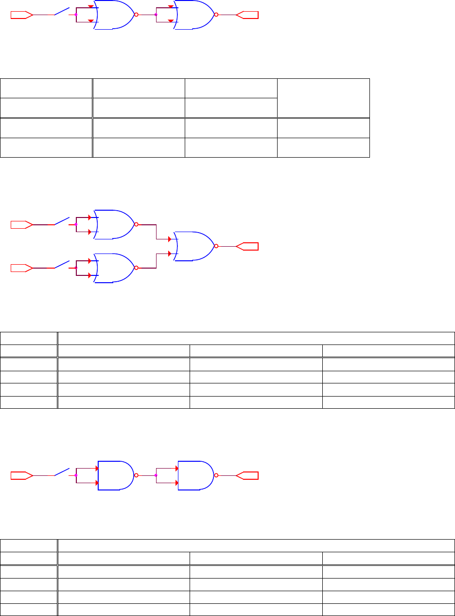
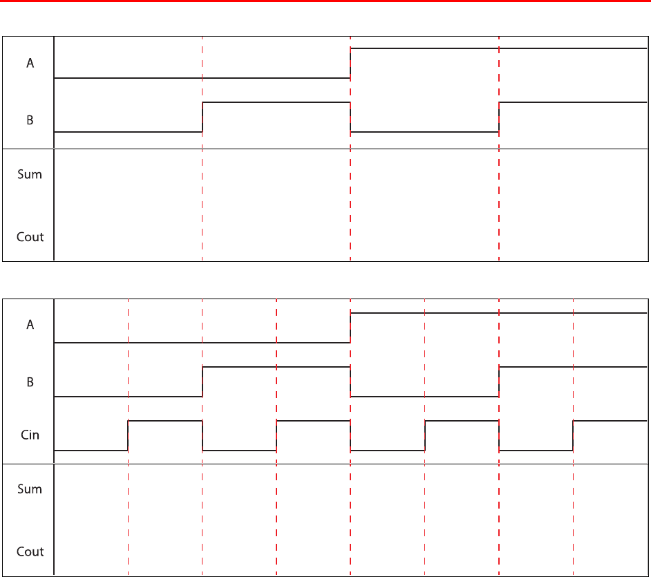
From the truth tables above, trace the output waveform for the half adder and full adder.
Figure 6. 1
Figure 6. 2

63
PROCEDURE
HALF ADDER IMPLEMENTATION
STARTING A NEW PROJECT
1. Create a new project by going to File > New > New Project….
2. In the New Project window, name your project and save it in a new folder.
3. In the Create PSPICE Project window, click Create a black project, then press OK.
ADDING LIBRARIES
4. Press Place > Part or press P to bring up the parts library.
Figure 6. 3
5. In Place Part window, click the Add Library icon, . In the folder, open the library called 7400, SOURCSTM.
Figure 6. 4

64
ADDING COMPONENTS TO SCHEMATIC
6. In the 7400 library, add the 7486 (XOR gate) and 7408 (AND gate) to the schematic.
Figure 6. 5
7. Place two DigStim1 parts on your schematic (one for each input). Double click on the “Implementation” text
and set the value to X and Y for each DigStim1.
8. Go to Place > Hierarchical Port… and place two PORTRIGHT-R ports to the left of the inputs of the XOR gate.
Double click on the “PORTRIGHT-R” text and rename each port X and Y for each port.
9. Go to Place > Hierarchical Port… and place one PORTLEFT-L port to the right of the output of the XOR gate.
Double click on the “PORTLEFT-L” text and rename it SUM.
10. Go to Place > Hierarchical Port… and place one PORTLEFT-L port to the right of the output of the AND gate.
Double click on the “PORTLEFT-L” text and rename it OUT.
11. Press W for the wire tool and connect each component together with wires. So far you should have the
following:
Figure 6. 6
CREATING A NEW SIMULATION PROFILE
12. Create a new simulation profile by pressing PSpice > New Simulation Profile or click the icon.
13. In the pop-up window type “halfadder-sim”. Press Create when done. Leave Inherit From as none.
14. A window called “Simulation Settings – lab1-sim” will pop-up. Set Run To Time to “1us”. This will make the
simulation run for 1us.
15. Next, click on Options > Gate Level Simulation > General and set DIGINITSTATE to 0 under the Value column.
Then press Apply, then OK.

65
CREATING A SIMULATION STIMULI
16. Click the DSTM1 symbol to select the part so that a purple dotted rectangle encloses the part.
Figure 6. 7
17. Right click on the DSTM1 symbol and click Edit PSpice Stimulus from the menu.
Figure 6. 8
18. A New Stimulus window will pop up with “X” already in the Name text field. In the Digital section, select Clock,
then press OK.
Figure 6. 9

66
19. In the Clock Attributes window, set Specify by to Period and on time. Set Period (sec) to 500ns and On time
(sec) to 250ns. Press Apply, then OK.
Figure 6. 10
20. Set another stimulus for Y, press Stimulus > New….
Figure 6. 11
Figure 6. 12

67
21. In the Clock Attributes window, set Specify by to Period and on time. Set Period (sec) to 250ns and On time
(sec) to 125ns. Press Apply, then OK.
22. Your Stimulus Editor should look like the following:
23. Press Save and press Yes to update schematic.
RUN SIMULATION
24. Place Voltage Level markers schematic by going to PSPICE > Markers > Voltage Level or press the icon.
The Voltage Level markers must be placed on the wires. Your schematic should look like the following:
Figure 6. 13
25. Press PSpice > Run or the icon to run simulation. Running the simulation will cause the Allegro PSpice
Simulator program to open which will contain a simulation of your schematic. It should look similar to the
screenshot below:
Figure 6. 14

68
26. Press Trace > Cursor > Display or press to enable the cursor. This will let you see the level of your signal.
Once enabled, left click and on your simulation to see the levels of your signal. You can click hold and drag as
well.
Figure 6. 15
27. Compare your simulated results with your pre-lab.
FULL ADDER IMPLEMENTATION
1. Open the halfadder project created in the previous section.
STARTING A NEW PROJECT
2. Create a new project by going to File > New > New Project….
3. In the New Project window, name your project as fulladder and save it in a new folder.
4. In the Create PSPICE Project window, click Create a black project, then press OK.
5. In the project file directory, right click PAGE1 and rename it as halfadder.
Before:
Figure 6. 16
After:
Figure 6. 17
ADDING LIBRARIES
6. The necessary libraries should already be added to your library list from implementing the halfadder. If not,
refer to step 4 in the from the previous section.

69
COPYING HALF ADDER TO SCHEMATIC
7. In the halfadder project, open the half adder schematic. Then left click drag over the halfadder until the entire
circuit is selected. All components will be highlighted in purple:
Note: Turn the schematic in Figure 6.18 into a block. To do so remove “DSTM1” and “DSTM2”, then copy to a
new schematic.
Figure 6. 18
8. Go to Edit > Copy or press Ctrl+C to copy the halfadder circuit.
9. Paste the halfadder circuit on to the new schematic named halfadder.
FULL ADDER SCHEMATIC
10. In the project file directory, right click fulladder.dsn and click on New Schematic…. Leave the schematic name
as the default, SCHEMATIC2.
Figure 6. 19
Figure 6. 20
11. Right click the SCHEMATIC2 folder created in the project directory and click New Page. Rename the new page
as fulladder.
Figure 6. 21

70
12. Set SCHEMATIC2 as root folder. Right click SCHEMATIC2 and click Make Root. This will move SCHEMATIC2 to
the top.
Before:
Figure 6. 22
After:
Figure 6. 23
13. Go to Place > Hierarchical Block…. In the Place Hierachical Block window, set Reference to halfadder1a,
Implementation Type to Schematic View, and Implementation name to SCHEMATIC1. Then press OK.
Figure 6. 24
Figure 6.

71
14. Left-click and drag to form a hierarchical box as shown below:
Figure 6. 25
15. Repeat step 12 and 13 to add another halfadder hierarchical block, however, name this one halfadder1b.
Figure 6. 26
16. Add the 7432 OR gate (7400 library), DigStim1 (X, Y, Cin), PORTRIGHT-R (X, Y, Cin), PORTRIGHT-L (Sum, Cout),
and wires to the schematic. Wire your circuit together as shown below:
Figure 6. 27
CREATING A NEW SIMULATION PROFILE
17. Create a new simulation profile by pressing PSpice > New Simulation Profile or click the icon.
18. In the pop-up window type “fulladder-sim”. Press Create when done. Leave Inherit From as none.
19. A window called “Simulation Settings – lab1-sim” will pop-up. Set Run To Time to “1us”. This will make the
simulation run for 1us.
20. Next, click on Options > Gate Level Simulation > General and set DIGINITSTATE to 0 under the Value column.
Then press Apply, then OK.

72
CREATING A SIMULATION STIMULI
21. Click the DSTM1 symbol to select the part so that a purple dotted rectangle encloses the part.
Figure 6. 28
22. Right click on the DSTM1 symbol and click Edit PSpice Stimulus from the menu.
Figure 6. 29
23. A New Stimulus window will pop up with “X” already in the Name text field. In the Digital section, select Clock,
then press OK.
Figure 6. 30

73
24. In the Clock Attributes window, set Specify by to Period and on time. Set Period (sec) to 1000ns and On time
(sec) to 500ns. Press Apply, then OK.
Figure 6. 31
25. Set another stimulus for Y, press Stimulus > New….
Figure 6. 32
26. Set Name to Y and Digital to Clock.
Figure 6. 33

74
27. In the Clock Attributes window, set Specify by to Period and on time. Set Period (sec) to 500ns and On time
(sec) to 250ns. Press Apply, then OK.
Figure 6. 34
28. Set another stimulus for Cin, press Stimulus > New….
Figure 6. 35
29. Set Name to Cin and Digital to Clock.
Figure 6. 36

75
30. In the Clock Attributes window, set Specify by to Period and on time. Set Period (sec) to 250ns and On time
(sec) to 125ns. Press Apply, then OK.
Figure 6. 37
31. Your Stimulus Editor should look like the following:
Figure 6. 38
32. Press Save and press Yes to update schematic.
RUN SIMULATION
33. Place Voltage Level markers schematic by going to PSPICE > Markers > Voltage Level or press the icon.
The Voltage Level markers must be placed on the wires. Your schematic should look like the following:
Figure 6. 39

76
34. Press PSpice > Run or the icon to run simulation. Running the simulation will cause the Allegro PSpice
Simulator program to open which will contain a simulation of your schematic. It should look similar to the
screenshot below:
Figure 6. 40
35. Press Trace > Cursor > Display or press to enable the cursor. This will let you see the level of your signal.
Once enabled, left click and on your simulation to see the levels of your signal. You can click hold and drag as
well.
Figure 6. 41
36. Compare your simulated results with your pre-lab.
BREADBOARD
1. Draw the gate level schematic of the full adder designed in part A, build it on a breadboard, and verify its
functionality.
2. Record the output in Table 6.3 and compare your results with Table 6.2.
Input
Output
A
B
C
in
C
out
Sum
0
0
0
0
0
1
0
1
0
0
1
1
1
0
0
1
0
1
1
1
0
1
1
1
Table 6. 3: Full adder truth table

77
Experiment 7: 2’s Complement Adder / Subtractor Circuit
OJECTIVES
After completing this experiment, you will be able to:
• Design, draw, construct, test, and demonstrate a 2s complement adder/subtractor system using only
7483 and 7486 ICs
MATERIALS NEEDED
• 7483 Four-bit adder IC
• 7486 Quad two-input XOR gate IC
• (4) LEDs
• (4) 330Ω resisters
THEORY
ADDER / SUBTRACTOR CIRCUIT
A 4-bit adder/subtractor circuit can be constructed using a 7483 4-bit binary full adder and a 7486 XOR gate IC. The
7483 IC performs the addition, while the 7486 IC is used to handle the subtraction operation. The 7483 IC has two
inputs for each of the four bits (A0, A1, A2, A3) and (B0, B1, B2, B3), and the carry-in (Cin) and carry-out (Cout)
lines.
Figure 7. 1
2’S COMPLEMENT
CONVERTING BETWEEN UNSIGNED AND SIGNED 2’S COMPLEMENT
In computing, the two's complement is a method used to represent signed integers. It allows both positive and
negative numbers to be stored and manipulated using the same binary arithmetic operations. In this
representation, the most significant bit (MSB) is used to represent the sign of the number, where 0 indicates a
positive number and 1 indicates a negative number.
To obtain the two's complement representation of a negative number, you follow these steps:
EXAMPLE 1: UNSIGNED TO 2’S COMPLEMENT
Let's find the two's complement representation of the decimal number -20 using 8-bit binary representation:
1. Write the digit as a positive unsigned binary number:
+20 = 00010100
78
2. Starting from the right-hand side and moving to the left, copy all the bits including the first ‘1’ reached:
Giving us: 00010100 → 100
3. Take the complement of the remaining bits:
Giving us: 00010 → 11101
Therefore, the two's complement representation of -20 in 8-bit binary is 11101100.
EXAMPLE 2: 2’S COMPLEMENT TO UNSIGNED
Now let’s convert back from the two's complement representation to the decimal representation:
4. Starting from the right-hand side and moving to the left, copy all the bits including the first ‘1’ reached:
Giving us: 11101100 → 100
1. Take the complement of the remaining bits:
Giving us: 11101 → 00010
2. Finally, interpret the result as a positive binary number:
+20 = 00010100
In this way, the two's complement representation allows us to perform arithmetic operations on signed integers
using the standard binary arithmetic operations.
ADDITION AND SUBTRACTION WITH 2’S COMPLEMENT
EXAMPLE 3: ADDITION
Let's add two numbers, 3 and -2, represented in 4-bit two's complement.
1. Represent the numbers in 4-bit binary form:
3 = 0011 (4-bit binary)
-2 = 2's complement of 2 (which is 0010) = 1110 (4-bit binary)
2. Add the binary numbers as if they were unsigned binary:
0011 (3)
+ 1110 (-2)
--------------
10001 (Carry-out)
3. Discard any overflow and keep the lower 4 bits of the result:
0001 (discard the carry-out)

79
4. Interpret the result as a signed decimal number:
0001 (4-bit binary) = 1 (decimal)
Therefore, the result of adding 3 and -2 using two's complement representation is 1.
EXAMPLE 4: SUBTRACTION
Let's subtract two numbers, 5 and 3, represented in 4-bit two's complement.
1. Represent the numbers in 4-bit binary form:
5 = 0101 (4-bit binary)
3 = 0011 (4-bit binary)
2. Find the two's complement of the number to be subtracted (3):
-3 (decimal) = -2's complement of 3 (which is 0011) = 1101 (4-bit binary)
3. Add the binary numbers as if they were unsigned binary:
0101 (5)
+ 1101 (-3)
--------------
10010 (Carry-out)
4. Discard any overflow and keep the lower 4 bits of the result:
0010 (discard the carry-out)
Step 5: Interpret the result as a signed decimal number:
0010 (4-bit binary) = 2 (decimal)
Therefore, the result of subtracting 3 from 5 using two's complement representation is 2.
In summary, two's complement allows us to perform addition and subtraction of signed integers using the same
binary arithmetic operations as for unsigned integers. It simplifies the calculations and representation of negative
numbers in computer systems.
PRELIMINARY PROCEDURE
1. Read the lab.
2. Design the 2s complement adder/subtractor system shown in Figure 7.2. Use a 7486 IC for the four XOR gates.
Use a single 7483 adder IC for the four full adders (FAs).
3. Number the pins on your design using the datasheets.

80
PROCEDURE
1. Circuit design:
Figure 7. 2
2. Find the sum of the following 4-bit 2’s compliment numbers:
Inputs
Outputs
A + B = S
Sum
Sum
LEDs,
Sum
4 + 3 = 7
0100
+
0011
=
0111
OFF
4
ON
3
ON
2
ON
1
-1 + -1 = -2
1111
+
1110
=
1 + -2 = -2
0001
+
1101
=
5 + -4 = 1
0101
+
1100
=
Table 7. 1
3. Find the difference of the following 4-bit 2’s complement numbers. The ‘+’ is not a typo:
Inputs
Outputs
A – B = D
Diff
Difference
LEDs,
Diff
7 – 3 = 4
0111
+
1101
=
0100
OFF
4
ON
3
OFF
2
OFF
1
-8 – 3 = -5
1000
+
0011
=
3 – -3 = 6
0011
+
0011
=
-4 – 2 = -6
1100
+
1110
=
Table 7. 2
R5
330
LED_S1LED_S2
R3
330
LED_S3
0
LED_S4
R4
330
LED_C
R1
330
R2
330
U1
7483A
A4
A3
A2
A1
B4
B3
B2
B1
C0
C4
SU M4
SU M3
SU M2
SU M1

81
EVALUATION AND REVIEW QUESTIONS
1. Draw an 8-bit 2’s Complement Adder/Subtractor circuit using two 7483 4-bit adder ICs and eight 7486
quad two-input XOR gate ICs. Build can test your circuit if you have the parts and time during lab.

82
Experiment 8: Multiplexers
OBJECTIVES
After completing this experiment, you will be able to:
• Use a multiplexer to construct a unsigned comparator, signed comparator, and a parity generator and
verify it’s functionality.
• Use and N-input multiplexer to implement a truth table containing 2N inputs.
• Troubleshoot a simulated failure in a test circuit.
MATERIALS NEEDED
• 74151A Data selector/multiplexer
• 7404 Hex inverter
• (1) 330Ω resister
• (1) LED
THEORY
MULTIPLEXERS
A multiplexer, often abbreviated as "mux," is a fundamental digital logic circuit used in electronics and digital
communications to select one of several input signals and forward it to a single output. In other words, a
multiplexer is a device that allows multiple digital signals to share a common communication channel.
The basic theory behind a multiplexer is that it uses control inputs to select one of several inputs to route to the
output. The number of inputs that a multiplexer can handle is determined by the number of control inputs that it
has. For example, a 2-to-1 multiplexer has two inputs and one control input, while a 4-to-1 multiplexer has four
inputs and two control inputs.
The operation of a multiplexer can be visualized as a set of switches that are controlled by the control inputs.
Depending on the state of the control inputs, the corresponding switch is closed, allowing the signal from the
corresponding input to pass through to the output.
Multiplexers are used in a wide range of digital systems, including computer memory systems, data
communication systems, and digital signal processing circuits. They are often used in conjunction with other digital
logic circuits, such as decoders and demultiplexers, to perform complex digital operations.
PRELIMINARY PROCEDURE
1. Read the lab.
2. Complete the truth table for each circuit.
3. Complete the circuit diagram corresponding to each truth table.
4. Number the pins on each circuit using the 7404 and 74151A datasheet.

83
PROCEDURE
2-BIT UNSIGNED COMPARATOR,
1. Build Figure 8.1 on a breadboard and verify your results with Table 8.1.
Input Output
Connect Data to:
A1 A0 B1 B0 Z
0 0 0 0 1
0 0 0 1 0
0 0 1 0
0 0 1 1
0 1 0 0
0 1 0 1
0 1 1 0
0 1 1 1
1 0 0 0
1 0 0 1
1 0 1 0
1 0 1 1
1 1 0 0
1 1 0 1
1 1 1 0
1 1 1 1
Table 8. 1: Truth table for 2-bit unsigned comparator,

84
Figure 8. 1
LED
74151A
Z
Z
E
I0
I1
I2
I3
I4
I5
I6
I7
S0
S1
S2
A0
5V
A1
B0
7404
330
B1

85
2-BIT SIGNED COMPARATOR,
2. Build Figure 8.2 on a breadboard and verify your results with Table 8.2.
Input Output
Connect Data to:
A1 A0 B1 B0 Z
0 0 0 0
0 0 0 1
0 0 1 0
0 0 1 1
0 1 0 0
0 1 0 1
0 1 1 0
0 1 1 1
1 0 0 0
1 0 0 1
1 0 1 0
(2 = 2) 1
1 0 1 1
(2 < 1) 0
1 1 0 0
1 1 0 1
1 1 1 0
1 1 1 1
Table 8. 2: Truth table for 2-bit signed comparator,

86
Figure 8. 2
LED
74151A
Z
Z
E
I0
I1
I2
I3
I4
I5
I6
I7
S0
S1
S2
A0
5V
A1
B0
7404
330
B1

87
EVEN PARITY GENERATOR
3. Build Figure 8.3 on a breadboard and verify your results with Table 8.3.
Input Output
Connect Data to:
A3 A2 A1 A0 Z
0 0 0 0 0
0 0 0 1 1
0 0 1 0
0 0 1 1
0 1 0 0
0 1 0 1
0 1 1 0
0 1 1 1
1 0 0 0
1 0 0 1
1 0 1 0
1 0 1 1
1 1 0 0
1 1 0 1
1 1 1 0
1 1 1 1
Table 8. 3: Truth table for even parity generator

88
Figure 8. 3
LED
A2
A0
330
74151A
Z
Z
E
I0
I1
I2
I3
I4
I5
I6
I7
S0
S1
S2
7404
A3
A1
5V

89
EVALUATION AND REVIEW QUESTIONS
1. Design a BCD invalid code detector using a 74151A. Show the connections for your design on Figure 8.4.
Figure 8. 4
2. Can you reverse the procedure of this experiment? That is, given the circuit, can you find the Boolean
expression? The circuit shown in Figure 8.5 uses 4:1 MUX. The inputs are called A2, A1, and A0. The first term
is obtained by observing that when both select lines are LOW, A2 is routed to the output; therefore, the first
minterm is written
. Using this as an example, find the remaining minterms.
=
+ _______________________________________________________________
Figure 8. 5
74151A
Z
Z
E
I0
I1
I2
I3
I4
I5
I6
I7
S0
S1
S2
330
0
5V
ZA
A1
A0
A2
U18
74153
ZA
ZB
S0
S1
EA
I0A
I1A
I2A
I3A
EB
I0B
I1B
I2B
I3B
90
3. Assume the circuit in Figure 8.1 had a short to ground on the output of the inverter. What effect would this
have on the output logic? What procedure would you use to find the problem?
4. Assume that the input to the 7404 in Figure 8.1 was open, making the output,
, a constant LOW. Which lines
on the truth table would give incorrect readings on the output?
5. How can both an even and old parity be obtained from the circuit in Figure 8.3?

91
Experiment 9: Demultiplexer
OJECTIVES
After completing this experiment, you will be able to
• Complete the design of a multiple output combinational logic circuit using a demultiplexer.
• Use an oscilloscope to develop a timing diagram for a counter-decoder circuit.
MATERIALS NEEDED
• 7408 Quad AND gate
• 7474 Dual D flip-flop
• 74LS139A decoder/demultiplexer
• LEDs: (2) red, (2) yellow, (2) green
• Resisters: (6) 330Ω, (2) 1.0kΩ
• Two oscilloscope probes
• One function generator probe
THEORY
DEMULTIPLEXER
A demultiplexer, also known as a " DMUX," is a digital circuit that takes in a single input and distributes it to
multiple outputs based on a control signal. The control signal specifies which output should receive the input data.
In a simple demultiplexer circuit, the input signal is connected to the decoder, which generates a binary code
based on the control signal. The binary code activates the corresponding switch, which directs the input signal to
the desired output. The other outputs are disabled, ensuring that the input signal is only received by the intended
output.
For most DMUXs, the selected output is LOW, whereas all others are HIGH. To implement a truth table that has a
single output variable with a decoder is not very efficient and is rarely done; however, a method for doing this is
shown conceptually in Figure 9.1. In this case, each line on the output represents one row on the truth table. If the
decoder has active-HIGH outputs, the output lines on the truth table with a 1 are ORed together, as illustrated in
Figure 9.1. The output of the OR gate represents the output function. If the outputs of the decoder are active-
LOW, the output lines with a 1 on the truth table are connected with a NAND gate. This is shown in Figure 9.2.
A DMUX is superior for implementing combinational logic when there are several outputs for the same set of input
variables. Each output line of the demultiplexer represents a line on the truth table. For active-HIGH decoder
outputs, OR gates are used, but a separate OR gate is required for each output function. Each OR gate output
represents a different output function. In the case of active-LOW decoder outputs, the OR gates are replaced by
NAND gates.

92
Figure 9. 1: Implementing a combinational logic function with an active HIGH DMUX.
Figure 9. 2: Implementing a combinational logic function with an active LOW DMUX.
PRELIMINARY PROCEDURE
• Complete the design of a multiple output combinational logic circuit using the demultiplexer in Figure 9.4.
• Number the pins on each circuit using the 74LS139A and 7474 datasheets.

93
PROCEDURE
SYNOPSIS
A digital controller is required to control traffic at an intersection of a busy main street and an occasionally used
side street. The main street is to have a green light for as long as there is no vehicle on the side street. The side
street is to have a green light until there is no vehicle on the side street. There is a caution light (yellow) between
changes from green to red on both the main street and the side street. These requirements are illustrated in the
pictorial diagram in Figure 9.3.
Figure 9. 3: Requirements for the traffic light sequence.
We will focus on combinational logic in this experiment. The key elements can be separated into a Gray-code
counter and a traffic light logic block. The traffic light logic block has two inputs (2-bit Gray-code) and must have an
output for each of the four states. The 74LS139A is a dual 2-line to 4-line decoder and will do the job nicely, so it is
selected.
The traffic light logic block logic takes the four 2-bit Gray-codes and must produce six outputs for activating the
traffic lights. A truth table for the traffic light is given in Table 9.1. The truth table is organized in Gray-code, which
is used by sequential logic to step through the states. The output logic must be active-LOW (0) to drive LEDs that
simulate the traffic lights.
State Code
Light Outputs
Main Street
Side Street
B
A
Red
Yellow
Green
Red
Yellow
Green
0
0
1/OFF
1/OFF
0/ON
0/ON
1/OFF
1/OFF
0
1
1/OFF
0/ON
1/OFF
0/ON
1/OFF
1/OFF
1
1
0/ON
1/OFF
1/OFF
1/OFF
1/OFF
0/ON
1
0
0/ON
1/OFF
1/OFF
1/OFF
0/ON
1/OFF
Table 9. 1: Truth table for the combinational logic. State outputs are active-LOW and light outputs are active-LOW.
TRAFFIC LIGHT COMBINATIONAL CIRCUIT
1. Build Figure 9.4 on a breadboard.
2. Complete Table 9.2 and compare your results with Table 9.1.

94
Figure 9. 4: Traffic light output logic.
State Code
Light Outputs
Main Street
Side Street
B
A
Red
Yellow
Green
Red
Yellow
Green
0
0
0
1
1
1
1
0
Table 9. 2: Experimental truth table
+5.0V
+5.0V
A
7408
Main y ellow
330
330
+5.0V
330
7408
330
330
Main green
74LS139A
G
A
B
Y0
Y1
Y2
Y3
330
Side red
B
Side y ellow
0
Main red
+5.0V
Side green
+5.0V
+5.0V

95
GREY-CODE SEQUENCER
3. Although you have not studied counters yet, the Gray-code counter shown in Figure 9.5 is simple to build and
is the basis of the sequential logic in the traffic signal control logic. Construct the counter and connect the
counter outputs to the select inputs of the 74LS139A (switches should be removed). The select inputs are
labeled B and A on the 74LS139A.
Figure 9. 5: Gray-code counter for sequencing the traffic signal decoder.
RESULTS
4. Use an oscilloscope to develop a timing diagram for the counter-decoder traffic light circuit. Set the function
generator to 10Hz.
Figure 9. 6: Timing Diagram

96
EVALUATION AND REVIEW QUESTIONS
1. Assume you needed an 8-bit decoder, but all that is available is a dual 74LS139A. Show how you could use it,
along with an inverter, to form an 8-bit decoder. (Hint: Consider using the enable inputs.)
2. Why were the AND gates in Figure 9.2 drawn as negative-NOR gates?
3. What is the advantage of Gray-code for the state sequence?
4. For the circuit in Figure 9.4, what symptom would you obverse if:
a. The B select input were open?
b. The B select input were shorted to ground?
c. The enable (G
) input were open?
5. How would the circuit be affected if instead of a Gray-code counter, you had a binary counter with the
sequence 00-01-10-11?

97
Experiment 10: D Latch and D Flip-Flop
OJECTIVES
After completing this experiment, you will be able to
• Demonstrate how a latch can debounce a switch.
• Construct and test a gated D latch from four NAND gates and an inverter.
• Test a D flip-flop and investigate serval applications circuits for both the latch and the flip-flop.
MATERIALS NEEDED
• Red LED
• Green LED
• 7486 quad XOR gate
• 7400 quad NAND gate
• 7404 hex inverter
• 7474 dual D flip-flop
• Resisters: two 330Ω, and two 1.0kΩ
THEORY
D LATCH AND D FLIP-FLOP
As you have seen, combinational logic circuits are circuits in which the outputs are determined fully by the inputs.
Sequential logic circuits contain information about previous conditions. The difference is that sequential circuits
contain memory and combinational circuits do not.
The basic memory unit is the latch, which uses feedback to lock onto and hold data. It can be constructed from two
inverters, two NAND gates, or two NOR gates. The ability to remember previous conditions is easy to demonstrate
with Boolean algebra. For example, Figure 8.1 shows an S-R latch made from NAND gates. This circuit is widely
used for switch debouncing and is available as an integrated circuit containing four latches (the 74LS279A).
A simple modification of the basic latch is a circuit is called a gated D (for Data) latch. An enable input allows data
present on the D input to be transferred to the output when Enable is asserted. When the enable input is not
asserted, the last level of Q and Q is latched. This circuit is available in integrated circuit form as the 7475A quad D
latch. Although there are four latches in this IC, there are only two shared enable signals.
Design problems are often simplified by having all transitions in a system occur synchronously (at the same time)
by using a common source of pulses to cause the change. This common pulse is called a clock. The output changes
occur only on either the leading or the trailing edge of the clock pulse. Some ICs have inputs that directly set or
reset the output any time they are asserted. These inputs are labeled asynchronous inputs because no clock pulse
is required. The D-type flip-flop with positive edge-triggering and asynchronous inputs is the 7474. In this
experiment, you will also test this IC.
PRELIMINARY PROCEDURE
1. Read the lab.
2. Number the pins on each circuit using their datasheet.

98
PROCEDURE
-
LATCH
1. Build the
-
l
atch shown in Figure 10.1.
Figure 10. 1:
-
latch
2. Use a wire to ground either input A or B. The LEDs will be used in this section as logic monitors. Since TTL logic
is much better at sinking current than at sourcing current, the LEDs are arranged to be ON when the output is
LOW (0). Therefore, a HIGH (1) corresponds to an LED being OFF.
+5.0V
+5.0V
B
1k
U1A
7400
+5.0V
A
R1
1k
1k
0
R2
1k
Red LED
Reads Q when ON
Use wire for switch
Green LED
Read Q Bar when ON
+5.0V
U1B
7400
4
5
6

99
3. Complete the truth table in Table 10.1.
Inputs Outputs LEDS
Q Q’ Green Red
1 0
1 1
0 1
1 1
0 0
Table 10. 1: Truth table for the
-
latch
D LATCH
4. Modify the basic S -R latch into a D latch circuit shown in Figure 10.2.
Figure 10. 2: D Latch
5. Connect the D input to a pulse generator set to 1 Hz, 5Vpp, 2.5V DC off-set. Connect the enable input to a
HIGH (through a 1.0 kΩ resistor). Observe the output; then change the enable to a LOW.
+5.0V
+5.0V
Green LED1
Reads Q Bar when ON
1k
7400
1k
1k
0
7400
Red LED1
Reads Q when ON
7400
7400
+5.0V
7404
V1

100
6. Complete the truth table in Table 10.2.
Inputs Outputs LEDS
En D Q Q’ Green Red
0 1
0 0
1 1
1 0
Table 10. 2: Truth table for D Latch

101
D Latch – Burglar Alarm
7. Now make a simple burglar alarm shown in Figure 10.3.
Figure 10. 3: D Latch - Burglar Alarm
8. The data input is represented by a switch connected to a window or door. The enable input is pulled HIGH
when the system is activated or LOW for standby. To reset the system, put a momentary ground on the Q
output as shown. Open the switch to confirm your alarm is working properly.
9. Complete the truth table in Table 10.3.
Inputs Outputs LEDS
En D Q Q’ Red
0 1
0 0
1 1
1 0
Table 10. 3: Truth table for D Latch - Burglar Alarm
330
7400
Enable
7404
0
Ready
7400
Switch:
(Doors, Windows, etc.)
+5.0V
7400
7400
Red LED
Alarm Indicator
0
0
+5.0V
Reset
1k
Standby
1k

102
THE D FLIP-FLOP
10. Construct the circuit shown in Figure 10.4. Connect the CLK input to a pulse generator set to 1 kHz, 5Vpp, 2.5V
DC off-set.
Figure 10. 4: D Flip-Flip
11. Connect the clock through the delay circuit. The purpose of the delay is to allow setup time for the D input.
Observe both the delayed clock signal and the Q output signal on a two-channel oscilloscope. View the
delayed clock signal on channel 1 and trigger the scope from channel 1. You should observe a dc level on the
output (channel 2). Sketch the wave form on Figure 10.5.
Figure 10. 5: Wave form for part b.
7404
7474
CLK
CLR
D
PRE
Q
Q
7404
0
+5.0V
+5.0V
Pulse Generator
7404
7404
1k
1k

103
12. Now remove the clock delay by connecting the clock input directly to the pulse generator. The output dc level
should have changed because there is insufficient setup time. Sketch the wave form on Figure 8.6.
Figure 10. 6: Wave form for part c.
13. Leave the clock delay circuit in place but disconnect the D input. Attach a wire from Q to the D input. Observe
the waveforms on a scope. Normally, for relative timing measurements, you should trigger the scope using the
channel that has the slowest waveform as the trigger channel. Sketch the wave form on Figure 8.7
Figure 10. 7: Wave form for part d.
14. Determine if
and
are synchronous or asynchronous inputs.
The
and
on the 7474 D flip-flop IC are _________________________ inputs.

104
PARITY TEST CIRCUIT
15. Construct the circuit shown in Figure 10.8. Connect the D input to a pulse generator set to 1 Hz, 5Vpp, 2.5V DC
off-set.
Figure 10. 8: Parity Test Circuit
16. This is a parity test circuit that takes serial data (bits arriving one at a time) and performs an exclusive-OR on
the previous result. The data are synchronous with the clock; that is, for every clock pulse a new data bit is
tested. Move the data switch to either a HIGH or a LOW prior to the clock pulse and observe the result.
Green LED
Ev en Parity Indicator
Clock Indicator
330
Red LED
Odd Parity Indicator
Wire Switch
330
+5.0V
330
1k
+5.0V
0
0
0
1k
1k
U15A
7486
+5.0V
7474
CLK
CLR
D
PRE
Q
Q
+5.0V
+5.0V

105
17. Complete the truth table in Table 10.4.
Inputs Outputs LEDS
Wire Switch D Q Q’ Green Red
0 1
0 0
1 1
1 0
Table 10. 4: Truth Table for the Parity Test Circuit

106
EVALUATION AND REVIEW QUESTIONS
1. Explain why the circuit in Figure 10.1 can be used to switch debounce a switch.
2. Could NOR gates be used for debouncing a switch? Explain.
3. Show how the burglar alarm of in part C could be constructed with one fourth of a 7475A D latch.
Figure 10. 9
4. The burglar alarm could be constructed with two cross-coupled NOR gates. Complete the circuit so that it has
the same functions as the alarm in part C (normally closed switches, alarm, and reset).
Figure 10. 10
5. Assume that the burglar alarm in Figure 10.3 does not function correctly. The Enable switch is in the Ready
position but the LED does not come on when one of the switches is open. Suggest at least 3 causes for this
failure. Circle the reason you think is most likely.
6. The serial parity test circuit in Figure 10.8 uses a D flip-flop. Why wouldn’t a D latch work just as well?
7475A
D
Q
EN
Q
7402
7402

107
Experiment 11: J-K Flip-Flop
OJECTIVES
After completing this experiment, you will be able to
• Test various configurations for a J-K flip-flop, including the asynchronous and synchronous inputs.
• Observe frequency division characteristics in the toggle mode.
• Measure the propagation delay of a J-K flip-flop.
MATERIALS NEEDED
• 74LS76 or 7476 dual J-K flip-flop
• LEDs: one red, one green, one yellow
• Resistors: seven 330Ω, four 1.0 kΩ
THEORY
JK FLIP-FLOPS
A JK flip-flop is a type of sequential logic circuit that can store one bit of information, also known as a "binary digit"
or "bit". It has two inputs: J (set) and K (reset), and two outputs: Q (the normal output) and Q' (the inverse output).
When both inputs J and K are at logic level 0 (low), the output state of the flip-flop remains unchanged. When J is
set to 1 (high) and K is at 0, the output state of the flip-flop changes to 1, and stays in that state until the inputs are
changed again. Conversely, when K is set to 1 and J is at 0, the output state of the flip-flop changes to 0, and
remains in that state until the inputs are changed again.
When both J and K inputs are set to 1, the output state of the flip-flop toggles. That is, if the output was 0, it
becomes 1, and if the output was 1, it becomes 0.
The toggle function of the JK flip-flop is particularly useful for creating frequency dividers, binary counters, and
other circuits where it is desirable to alternate between two states.
In summary, a JK flip-flop operates by changing its output state based on the combination of inputs J and K, and
can store one bit of information at a time. The truth table for a JK flip-flop is shown in table 9.1.
Input Output
CLK J K Q Q’
L H X X X 1 0
H L X X X 0 1
H H CP 0 0 Memory
H H CP 0 1 0 1
H H CP 1 0 1 0
H H CP 1 1 Toggle
Table 11. 1: JK Truth Table (CP = Clock Pulse)

108
PRELIMINARY PROCEDURE
1. Read the lab.
2. Review the J-K flip-flop and number the pins on Figure 11.1, 11.2, 11.3, and 11.4.
PROCEDURE
PART I
1. Construct the circuit shown in Figure 11.1. The LEDS are logic monitors and are ON when their outputs are
LOW.
Figure 11. 1
2. Set
and
to HIGH (1). Set CLK to LOW (0), so that it’s not active. Select the “set” mode by setting J = 1
and K = 0.
a) Now test the effects of
and
by putting a logic 0 on each, one at a time. Are preset and clear
inputs synchronous or asynchronous?
3. With the JK flip-flop still in the “set” mode, put
HIGH (1) and
to LOW (0), then pulse the clock by
flipping the clock switch from 1 to 0 (Note the bubble at the input of the clock). Observe that the
input
overrides the J input.
4. Determine what happens if both
and
are connected to a LOW (0) at the same time. Summarize your
observations in your report.
330
CLK
330
+5.0V
CLR Bar
J
+5.0V
7476
PRE
J
CLK
K
CLR
Q
Q
Green
R's= 330
Red
K
PRE Bar
0

109
PART II
5. Construct the circuit shown in Figure 11.2. Connect the function generator to the clock input and set it to a 5V
1 Hz square wave with a DC offset of 2.5V. Add an LED clock indicator to the function generator so that you
can observe the clock pulse and the outputs at the same time.
Figure 11. 2
6. Test all four combinations of J and K inputs while observing the LEDs. Is data transferred to the output on the
leading or the trailing edge of the clock? Complete Table 11.2.
Input Output
J K Q Q’ Red LED Green LED
1 0
0 1
1 1
0 0
Table 11. 2: Experimental JK flip-flop truth table
7. Summarize your observations in the report. Include a discussion of the truth table for the J-K flip-flop.
330
R's= 330
K
PRE Bar
0
Clock Indicator
+5.0V
330
7476
PRE
J
CLK
K
CLR
Q
Q
CLR Bar
Function
Generator
J
+5.0V
Green
0
Red
330
0

110
PART III
8. Construct the circuit shown in Figure 11.3. Connect the function generator to the clock input and set it to a 5V
5 Hz square wave with a DC offset of 2.5V.
Figure 11. 3
9. Complete Table 11.3 and summarize your observations in your report.
Current State Next State
J =
K = Q Red LED Green LED
J =
K = Q Red LED Green LED
1 0
0 1
Table 11. 3: Current state, next state
PART IV
7476
PRE
J
CLK
K
CLR
Q
Q
330
Green
Function
Generator
330
Red
330
Clock Indicator
330
+5.0V
330
0
+5.0V
+5.0V

111
10. An application of the toggle mode is found in certain counters. Cascaded flip-flops can be used to perform
frequency division in a circuit called a ripple counter. Figure 11.4 illustrates a ripple counter using the two flip-
flops in the 74LS76 IC.
11. Construct the circuit shown in Figure 11.4. Connect the function generator to the clock input and set it to a 5V
1 Hz square wave with a DC offset of 2.5V. Notice that when an LED is ON, the Q output is HIGH. The red and
green LEDs indicate that the pulse generator frequency has been changed by the flip-flops.
Figure 11. 4
12. Sketch the QA and QB output on Figure 11.5.
Figure 11. 5
Red
Green
1k
330
330
330
QB
Clock Indicator
+5.0V
QA
+5.0V
Function
Generator
7476
PRE
J
CLK
K
CLR
Q
Q
A
0
7476
PRE
J
CLK
K
CLR
Q
Q
+5.0V
B
+5.0V
1k

112
EVALUATION AND REVIEW QUESTIONS
1. What is the difference between an asynchronous and a synchronous input?
2. Describe how you would set a J-K flip-flop asynchronously.
3. How would you set it synchronously?
4. If both J and K inputs are LOW and PRE and CLR are HIGH, what effect does the clock have on the output of a J-
K flip-flop?
5. Assume a student accidentally reversed the J and K inputs on the circuit in Figure 11.3. What effect would be
observed?
6. Assume the red LED in Figure 11.3 is on steady and the green LED is off. The yellow LED is blinking. What are
three possible troubles with the circuit?
7. Assume the green LED in Figure 11.4 is off but the red LED is blinking. A check at the CLK input of the second
flip-flop indicates clock pulses are present. What are possible troubles with the circuit?

113
Experiment 12: Asynchronous Counter
OJECTIVES
After completing this experiment, you will be able to
• Build and analyze asynchronous up and down counters.
• Change the modulus of a counter.
• Use an IC counter and truncate its count sequence.
MATERIALS NEEDED
• 7400 quad NAND gates
• 7474 dual D flip-flop
• 7493A binary counter
• 7486 quad XOR gate
• Two LEDs
• Resisters: two 330Ω, two 1.0 kΩ
THEORY
ASYNCHRONOUS COUNTERS
Digital counters are classified as either synchronous or asynchronous, depending on how they are clocked.
Synchronous counters are made from a series of flip-flops that are clocked together. By contrast, asynchronous
counters are a series of flipflops, each clocked by the previous stage, one after the other. Since all stages of the
counter are not clocked together, a “ripple” effect propagates as various flip-flops are clocked. For this reason,
asynchronous counters are called ripple counters. You can easily make a ripple counter from D or J-K flip-flops by
connecting them in a toggle mode.
The modulus of a counter is the number of different output states the counter may take. The counters you will test
in the first four steps of this experiment can represent the numbers 0, 1, 2, and 3; therefore, they have a modulus
of 4.
Two methods for changing a counter from up to down or vice versa are illustrated in this experiment. The first
method involves moving the logical “true” output of the counter to the other side (as illustrated in Figures 10.2
and 10.3). The second method changes the way the counter is triggered.
If we tabulate a binary count sequence, we note that the LSB (least significant bit) changes at the fastest rate and
the rate of change is divided by 2 as we look at succeeding columns. A typical 3-Stage counter might have output
waveforms as shown in Figure 10.1. For this counter, we can assign each output with a “weight” equal to the
column value that would be assigned to binary numbers. Output QA has a weight of 1, output QB has a weight of
2, and output QC has a weight of 4. For the counter shown, the count sequence is for an up counter.

114
Figure 12. 1
For most applications requiring a counter, MSI counters are available. The 7493A is an example of an asynchronous
counter containing four J-K flip-flops, with the J and K inputs internally wired HIGH, putting them in the toggle
mode. Three of the flip-flops are connected as a 3-bit counter. The fourth flip-flop is separate, including its own
clock input. To form a 4-bit counter, connect the QA output of a single J-K flip-flop to the clock B input of the 3-bit
counter. A common reset line goes to all flip-flops. This reset line is controlled by an internal 2-input NAND gate.
You can select any count sequence up to 16 by choosing the internal counter, detecting the desired count, and
using it to reset the counter. In the For Further Investigation section, you will be introduced to an idea for changing
the up/down count sequence using a control signal.
PRELIMINARY PROCEDURE
1. Read the lab.
2. Review asynchronous counters and number the pins on Figure 10.2, 10.3, 10.4, 10.5, 10.6, 10.7, 10.8, and
10.9.

115
PROCEDURE
Note: The LED indicators in this experiment are connected through NAND gates wired as inverters to form the
display portion of the circuit. Although not strictly necessary, this method enables you to more easily visualize the
ideas presented in the experiment.
PART I
1. Construct the 2-bit asynchronous counter shown in Figure 12.2. Clock flip-flop A using a 5V 1 Hz square wave
(2.5V DC offset) from the function generator to the clock input and watch the sequence on the LEDs.
Figure 12. 2
2. Speed up the generator to 1 kHz and view the A and B output waveforms on a dual-channel oscilloscope. If
the clock frequency is not stated in other parts, use 1 kHz to view signals on the oscilloscope. Trigger the
oscilloscope from channel 1 while viewing the B signal on channel 1 and the A signal or the clock on channel 2.
Sketch the output timing diagram in Figure 12.3.
Figure 12. 3
3. By observation of your waveforms, determine whether this is an up counter or a down counter, and record
your answer.
+5.0V
1k
330
7474
CLK
CLR
D
PRE
Q
Q
+5.0V
330
CLK
A
7400
LED
1k
B
7400
+5.0V
7474
CLK
CLR
D
PRE
Q
Q
+5.0V
LED

116
PART II
4. Now we will change the way we take the “true” output from the counter and see what happens. If logic
“truth” is taken from the other side of each flip-flop, then we have the circuit shown in Figure 12.4.
Figure 12. 4
5. Modify your circuit and view the output waveform from each stage. Sketch the timing diagram on Figure 12.5
of the report.
Figure 12. 5
6. By observation of your waveforms, determine whether this is an up counter or a down counter, and record
your answer.
+5.0V
CLK
1k
+5.0V
LED
7400
B
+5.0V
A
1k
LED
7474
CLK
CLR
D
PRE
Q
Q
330
+5.0V
330
7474
CLK
CLR
D
PRE
Q
Q
7400

117
PART III
7. Next, we will change the manner in which flip-flop B is clocked. Change the circuit to that of Figure 12.6.
Figure 12. 6
8. The “true” output of the counter remains on the
side of the flip-flops. View the outputs as before and
sketch the waveforms on Figure 12.7.
Figure 12. 7
9. By observation of your waveforms, determine whether this is an up counter or a down counter, and record
your answer.
LED
7400
+5.0V
LED
+5.0V
1k
330
7474
CLK
CLR
D
PRE
Q
Q
CLK
330
7400
1k
7474
CLK
CLR
D
PRE
Q
Q
B
A
+5.0V
+5.0V

118
PART IV
10. Now change the logic “true” side of the counter, but do not change the clock, as illustrated in Figure 12.8.
Figure 12. 8
11. Again, sketch the outputs of each flip-flop on Figure 12.9.
Figure 12. 9
12. By observation of your waveforms, determine whether this is an up counter or a down counter, and record
your answer.
LED
7400
+5.0V
+5.0V
CLK
LED
+5.0V
330
330
1k
7400
B
7474
CLK
CLR
D
PRE
Q
Q
1k
A
7474
CLK
CLR
D
PRE
Q
Q
+5.0V

119
PART V
13. You can change the modulus of the counter by taking advantage of the asynchronous clear (CLR
) and
asynchronous preset (PRE
) inputs of the 7474. Look at the circuit of Figure 12.10, a modification of the circuit
in Figure 10.5. Predict the behavior of this circuit, and then build the circuit.
Figure 12. 10
14. Set the clock frequency at 500 kHz and look for the very short spike that causes the count sequence to be
truncated. Sketch the output waveforms of each flip-flop on 12.11 and determine the count sequence.
Figure 12. 11
15. By observation of your waveforms, determine whether this is an up counter or a down counter, and record
your answer.
LED
A
+5.0V
330
330
7400
1k
7474
CLK
CLR
D
PRE
Q
Q
+5.0V
7400
B
CLK
LED
7400
7474
CLK
CLR
D
PRE
Q
Q
+5.0V

120
PART VI
16. You can configure the 7493A 4-bit binary counter to count from 0 to 15 by connecting the output of the single
flip-flop (QA) to the clock B input. Connect the function generator to the clock A input. From the data sheet,
determine the necessary connections for the reset inputs.
Figure 12. 12
17. Set the clock for 400 kHz. Trigger a two-channel oscilloscope from the lowest-frequency symmetrical
waveform (QD), and observe, in turn, each output on the second channel. Sketch the timing diagram on Figure
12.13.
Figure 12. 13
A
B
CLK
D
C
7493A
CKA
CKB
R01
R02
QA
QB
QC
QD

121
PART VII
18. Figure 12.14 shows a 7493A counter configured with a truncated count sequence. Modify your previous circuit
(Figure 12.13) and observe the output waveforms on an oscilloscope. Again, trigger the oscilloscope on the
lowest-frequency symmetrical waveform, and observe each output on the second channel.
Figure 12. 14
19. Sketch the timing diagram on Figure 12.15.
Figure 12. 15
20. By observation of your waveforms, determine whether this is an up counter or a down counter, and record
your answer.
CLK
A
B
C
D
7493A
CKA
CKB
R01
R02
QA
QB
QC
QD

122
EVALUATION AND REVIEW QUESTIONS
1. Figure 12.16 shows a digital oscilloscope display for the circuit in Figure 10.4, but with a different clock
frequency. The upper signal is B on CH1. The lower signal is A on CH2.
a) What is the clock frequency?
b) Why is it best to trigger the scope on CH1?
Figure 12. 16
2. Explain how the count sequence of a ripple counter can be truncated.
a) Why does the procedure produce a glitch?
3. Suppose that the counter in Figure 12.4 has both LEDs on all the time. The clock is checked and found to be
4. present. What possible faults would cause this condition?
5. Why shouldn’t you trigger your oscilloscope from the clock when determining the time relationship of the
outputs of a counter?
6. Draw the circuit for a 7493A configured as a modulus-9 counter.
a) Sketch the waveforms you would see from the circuit.
Figure 12. 17
7. Assume the 7493A in Figure 12.12 were replaced with a 7492A and wired the same way. Referring to the
count sequence shown on the data sheet, determine the modulus and count sequence of the circuit.

123
Experiment 13: Analysis of Synchronous Counters with Decoding
OJECTIVES
After completing this experiment, you will be able to:
• Analyze the count sequence of synchronous counters using a tabulation method.
• Construct and analyze a synchronous counter with decoding. Draw the state diagram.
• Use an oscilloscope to measure the time relationship between the flip-flops and the decoded output.
• Explain the concept of patrial decoding.
MATERIALS NEEDED
• Two 7476 dual J-K flip-flops.
• 7400 quad NAND gates.
• Two SPST N.O. pushbutton (N.O. means Normally Open).
• Four LEDs.
• Resistors: four 330Ω, two 1.0kΩ.
THEORY
SYNCHRONOUS COUNTERS
Synchronous counters have all clock lines tied to a common clock, causing all flip-flops to change at the same time.
For this reason, the time from the clock pulse until the next count transition is much faster than in a ripple counter.
This greater speed reduces the problem of glitches (short, unwanted signals due to non-synchronous transitions) in
the decoded outputs. However, glitches are not always eliminated because stages with slightly different
propagation delays can still have short intermediate states. One way to eliminate glitches is to choose a Gray code
count sequence (only one flip-flop transition per clock pulse).
Decoding is the “detecting” of a specific number. A counter with full decoding has a separate output for each state
in its sequence. The decoded output can be used to implement some logic that performs a task. The decoded
outputs are also useful for developing counters with irregular count sequences. This experiment will also introduce
you to partial decoding, a technique that allows you to decode the output with less than all the bits.
Several MSI counters are available with features on one chip, such as synchronous and asynchronous preset or
clear, up/down counting, parallel loading, display drivers, and so on. If it is possible to use an MSI counter for an
application, this choice is generally the most economical. If it is not possible, then you must design the counter to
meet the requirement. In this experiment you will analyze already designed synchronous counters step by step. In
the next experiment, you will design a counter to meet a specific requirement.

124
HOW TO ANALYSIS PRE-DESIGNED SYNCHRONOUS COUNTERS
The method for analyzing a synchronous counter is a systematic tabulation technique. This method is illustrated
for the counter shown in Figure 13.1. Begin by setting up Table 13.1. The table lists the outputs and inputs for each
flip-flop in the counter.
Figure 13. 1
1. Write the equations for the J and K inputs of each counter using the schematic shown in Figure 11.1. The
equations are shown in Table 13.1.
2. Assume an initial state for the counter. In this example, let’s arbitrarily choose 0000
2
.
Complete the first row by determining each J and K input. The equations (Step 1) and the inputs 0000
2
are used to
compute the binary value of J and K.
Table 13. 1

125
3. Use the J-K truth table to determine the next state of each flip-flop. In this example, J
D
= K
D
= 0 means Q
D
will
not change; also notice that Q
C
and Q
B
will not change. However, J
A
= 1, K
A
= 0 means Q
A
= 1 after the next
clock pulse. Write the next state under the present state that was originally assumed.
Table 13. 2
4. Continue until all possible inputs are accounted for. This is demonstrated in Table 13.2. The sequence can now
be shown on a state diagram, as in Figure 13.2.
Figure 13. 2
The analysis continues along these lines until all possible (2
N
) states have been considered, including states that are
not in the main count sequence. The completed table is shown as Table 13.2. Using the information from the table,
the complete state diagram can then be drawn as illustrated in Figure 13.2. This completely describes the
operation of the counter. This counter has an interesting and somewhat unusual application. It is used to develop
the proper sequence of signals necessary to half-step a stepper motor.

126
PRELIMINARY PROCEDURE
1. Review synchronous counters and read the lab.
2. Number the pins on Figure 13.3, 13.4, and 13.5.
3. Complete Table 13.2 and draw the state diagram. Examine the counter shown in Figure 13.3. Since there are
two flip-flops, there are four possible output states. Analyze the sequence by completing Table 13.2 using the
method illustrated in the Theory section. From the table, draw the predicted state diagram.
Output
Inputs
Q
B
Q
A
J
B
=
K
B
=
J
A
=
K
A
=
Table 13. 3
4. Analyze the counter shown in Figure 13.5 by completing Table 13.3. Account for all possible states, including
unused states. If you correctly account for the unused states, you will see that all unused states return to state
2. Draw the state diagram.
Outputs
Inputs
Q
C
Q
B
Q
A
J
C
=
Kc
=
J
B
=
K
B
=
J
A
=
K
A
=
Table 13. 4

127
PROCEDURE
1. Build the synchronous counter circuit shown in Figure 13.3.
Figure 13. 3
2. Build the NAND gates circuits shown in Figure 13.4, which serve as state decoders with an active-LOW output
for each state. To avoid confusion, the lines from the counter to the decoders are not shown on the
schematic. Save the decoder circuits as they will be used with the next counter circuit in this lab.
3. Set the function generator to 5V, 2.5V
DC-Off-Set
, and 1Hz for the clock signal. Observe the order in which the
decoders LEDs are illuminated. Are they showing the correct sequence? If not, debug your circuit until the
decoder circuit shows the correct sequence.
4. Use an oscilloscope to measure Q
B
and Q
A
. Set the oscilloscope to trigger on channel 1 with the Q
B
signal. Set
channel to Q
A
and fit both signals on to the screen. Observe that your waveforms match the state sequence.
Photograph or save the oscilloscope screen on a USB drive for your report.
0
1k
0
+5.0V
Function Generator
1k
JK_A
7476
PRE
J
CLK
K
CLR
Q
Q
+5.0V
7476
PRE
J
CLK
K
CLR
Q
Q
1k
JK_B
+5.0V
0

128
Figure 13. 4
5. Assume that a failure has occurred in the circuit. The wire from the Q
B
output to K
A
has become open. What
effect does this open have on the output? Look at the signals on your oscilloscope and determine the new
state diagram. Add the state diagram to your report.
Q_B Bar
330
Q_B
+5.0V
Q_B
S_2 Bar
Q_A
7400
S_3 Bar
330
330
Q_B Bar
330
S_1 Bar
+5.0V
7400
S_0 Bar
Q_A Bar
7400
Q_A Bar
Q_A
7400
+5.0V
+5.0V

129
6. Modify the circuit by adding another flip-flop and changing the inputs to J
A
, K
A
, and J
B
, as shown in Figure 13.5.
Leave the 7400 decoder circuit but remove the set and clear switches/buttons. The decoder circuit will form
an example of partial decoding—a technique frequently employed in computers.
Figure 13. 5
7. Set the function generator (CLK) to 1 Hz and observe the LEDs connected to the state decoders. Notice that
state 4 is not in the main sequence but state 0 is in the main sequence of the counter. This means that every
time the state 0 LED turns ON, the counter is actually in state 0. This is an example of partial decoding; the
MSB was not connected to the decoder, yet there is no ambiguity for state 0 because state 4 is not possible.
Likewise, there is no ambiguity for state 0 or state 7, but partial decoding is not adequate to uniquely define
states 2 and 6.
+5.0V
0
JK_B
7476
PRE
J
CLK
K
CLR
Q
Q
JK_A
7476
PRE
J
CLK
K
CLR
Q
Q
1k
+5.0V
Function Generator
JK_C
7476
PRE
J
CLK
K
CLR
Q
Q
1k

130
EVALUATION AND REVIEW QUESTIONS
1. The counter used for half-stepping a stepper motor in the example of Figure 13.1 has a state diagram
sequence that is shown in Figure 13.2. Beginning with state 1, sketch the Q
D
, Qc, Q
B
, and Q
A
outputs. (Hint: An
easy way to start is to write the binary number vertically where the waveforms begin. This procedure is
started as an example.)
Figure 13. 6
2. Determine the sequence of the counter shown in Figure 13.7 and draw the state diagram.
Figure 13. 7
3. How could you incorporate full decoding into the counter circuit shown in Figure 13.5?
4. Explain the changes you would make to the circuit in Figure 13.5 in order to add a pushbutton that resets the
counter into state 2.
5. Assume a problem exists with the counter shown in Figure 13.3. The counter is “locked-up” in state 3. What
are two faults that can account for this problem?
6. Assume the synchronous counter in Figure 13.1 is “locked-up” in state 9. A quick check of power, ground, and
clock indicate they are all O.K. Which flip-flop is the likely cause of the problem? Why?

131
Experiment 14: Design of Synchronous Counters
OJECTIVES
After completing this experiment, you will be able to:
• Design a synchronous counter with up to 16 states in any selected order.
• Construct and test the counter. Determine the state diagram of the counter.
MATERIALS NEEDED
• (2) 7476 dual J-K flipflops
• 7408 quad AND gate or other SSI IC determined by the student’s design.
THEORY
DESIGNING SYNCHRONOUS COUNTERS
The design of a synchronous counter begins with a description of the state diagram that specifies the required
sequence. All states in the main sequence should be shown; states that are not in the main sequence should be
shown only if the design requires these unused states to return to the main sequence in a specified way. If the
sequence can be obtained from an already existing IC, this is almost always more economical and simpler than
designing a special sequence.
HOW TO DESIGN SYNCHRONOUS COUNTERS
From the state diagram, a next-state table is constructed. This procedure is illustrated with the example in Figure
20-1 for a simple counter and again in Figure 20-3 for a more complicated design. Notice in Figure 20-1 that the
next state table is just another way of showing the information contained in the state diagram. The advantage of
the table is that the changes made by each flip-flop going from one state to the next state are clearly seen. The
third step is to observe the transitions (changes) in each state. The required logic to force these changes will be
mapped onto a Karnaugh map. In this case, the Karnaugh map takes on a different meaning than it did in
combinational logic but it is read the same way. Each square on the map represents a state of the counter. In
effect, the counter sequence is just moving from square to square on the Karnaugh map at each clock pulse. To
find the logic that will force the necessary change in the flip-flop outputs, look at the transition table for the J-K
flip-flop, shown as Table 20-1. Notice that all possible output transitions are listed first; then the inputs that cause
these changes are given. The transition table contains a number of X’s (don’t cares) because of the versatility of
the J-K flip-flop, as explained in the text. The data from the transition table are entered onto the Karnaugh maps as
illustrated.
Assume you need to design a counter that counts 0-1-3-2 and stays in state 2 until a reset button is pressed. Two
flip-flops are required. Let Q
B
= MSB and Q
A
= LSB. Use a J-K flip-flop.
1. Draw a state diagram.
Figure 14. 1

132
2. Draw next-state table.
Table 14. 1
Table 14. 2
3. Determine inputs required for each flip-flop.
a) Read present state 00 on next-state table.
b) Note the Q
B
does not change 0 → 0 (present to next state) and Q
A
changes from 0 →1.
c) Read the required inputs to cause these results from transition Table 14.2.
d) Map each input from transition table onto Karnaugh map.
Figure 14. 2
e) Complete maps
Figure 14. 3
f) Read minimum logic from each map.
J
B
= Q
A
, K
B
= 0, J
A
=
, K
A
= Q
B

133
4. Draw circuit and check.
Figure 14. 4
When the maps are completed, the logic can be read from the map. This logic is then used to set up the circuit as
shown in Step 4 of Figure 20-1. It is a good idea to check the design by verifying that the count sequence is correct
and that there are no lock-up states. (A lock-up state is one that does not return to the main sequence of the
counter.) The design check can be done by completing a table such as Table 13.2 in the last experiment.
The design procedure just described can be extended to more complicated designs. In Experiment 13 a counter
was shown (Figure 13.1) that generates the required waveforms for half-stepping a stepper motor.

134
PRELIMINARY PROCEDURE
1. Read the lab.
2. A Gray code synchronous counter is often used in state machine design. This problem requires a six-state Gray
code counter. The usual Gray code sequence is not used because the sixth state would not be “Gray” when
the counter returns to zero. Instead, the sequence shown in Figure 14.5 is required. There are two unused
states: state 5 and state 7. For the initial design, these states are not shown. Complete the next-state table in
the report for the main sequence shown here.
Figure 14. 5
Present and Next State J-K Flop-Flop Inputs
Q
D
Q
C
Q
B
J
C
K
C
J
B
K
B
J
A
K
A
0
0
0
0
0
1
0
1
1
0
1
0
1
1
0
1
0
0
Table 14. 3
3. Using the transition table for the J-K flipflop, complete the Karnaugh maps shown in the report. The J-K
transition table (Table 14.2) is repeated in the report for convenience.
4. Read the required logic expressions from each map that you completed in preliminary procedure. Check that
the unused states return to the main sequence. If they do not, modify the design to assure that they do
return.

135
PROCEDURE
1. Construct and test your circuit. You can check the state sequence with an oscilloscope or a logic analyzer.
Summarize the results of your test in your report.
EVALUATION AND REVIEW QUESTIONS
1. Complete the design of the sequential counter in Figure 14.3 by constructing Karnaugh maps for the B and A
flip-flops. Read the maps. As a check, you can compare your result with the circuit drawn in Figure 14-1.
2.
Describe the logic necessary to add a seven-segment display to the circuit you designed in this experiment to
enable the display to show the state of the counter.
3.
Assume you wanted to make the sequential circuit you designed in this experiment start in state 6 if a reset
pushbutton is pressed. Describe how you would modify the circuit to incorporate this feature.
4.
Assume you wanted to change the circuit from this experiment to be able to reverse the sequence. How
would you go about this?
5.
Assume you wanted to trigger a one-shot (74121) whenever the circuit you designed went into state 2 or state
4. Explain how you could do this.
6.
Draw the transition table for a D flip-flop. Start by showing all possible output transitions (as in the J-K case)
and consider what input must be placed on D in order to force the transition.
a)
Why is the J-K flip-flop more versatile for designing synchronous counters with irregular sequences?

136
Appendix A

137
Appendix B
BREADBOARD
Figure 1.1
Figure 1.2
Figure 1.3
The breadboard has two basic internal connections, the vertical and horizontal. The verticals
are connected from top to bottom, if 5 volts is placed on the very first pin, 5 volts will be
present at the very last pin and any pin in between; this is demonstrated in Figure 1.2 from red
pin to red pin. The horizontal strips are connected by every 5 pins. Looking at Figure 1.3 pin A1
to E1 are connected internally.
